Hybrid material inversion mode gaa cmosfet

a technology of hybrid materials and inversion modes, applied in the direction of semiconductor devices, electrical apparatus, transistors, etc., can solve the problems of low leakage current, low carrier mobility, and degrade device performance, and achieve low low-frequency noise, high carrier mobility, and high carrier mobility

Inactive Publication Date: 2011-10-20
SHANGHAI INST OF MICROSYSTEM & INFORMATION TECH CHINESE ACAD OF SCI
View PDF5 Cites 28 Cited by
  • Summary
  • Abstract
  • Description
  • Claims
  • Application Information

AI Technical Summary

Benefits of technology

[0010]The device structure according to the prevent invention is quite simple, compact and highly integrated. In an inversion mode, the devices have high carrier mobility, low low-frequency noises. Meanwhile, polysilicon gate depletion and short channel effects are prevented, and the threshold voltages of the devices are increased.

Problems solved by technology

As the device size continues to shrink, a major challenge in scaling down the channel length is to maintain a high current drive capability (Ion) and a stable threshold voltage, and control the device leakage current (Ioff) at the same time.
Short channel effect (SCE) degrades device performance and is a severe obstacle to scale down the channel length.
The drawback of this technology is that the PMOS device fabricated in the epitaxial layer is not isolated from the substrate with buried oxide and thus the leakage current will be high.

Method used


Image

  • Hybrid material inversion mode gaa cmosfet
  • Hybrid material inversion mode gaa cmosfet
  • Hybrid material inversion mode gaa cmosfet

Examples


first embodiment

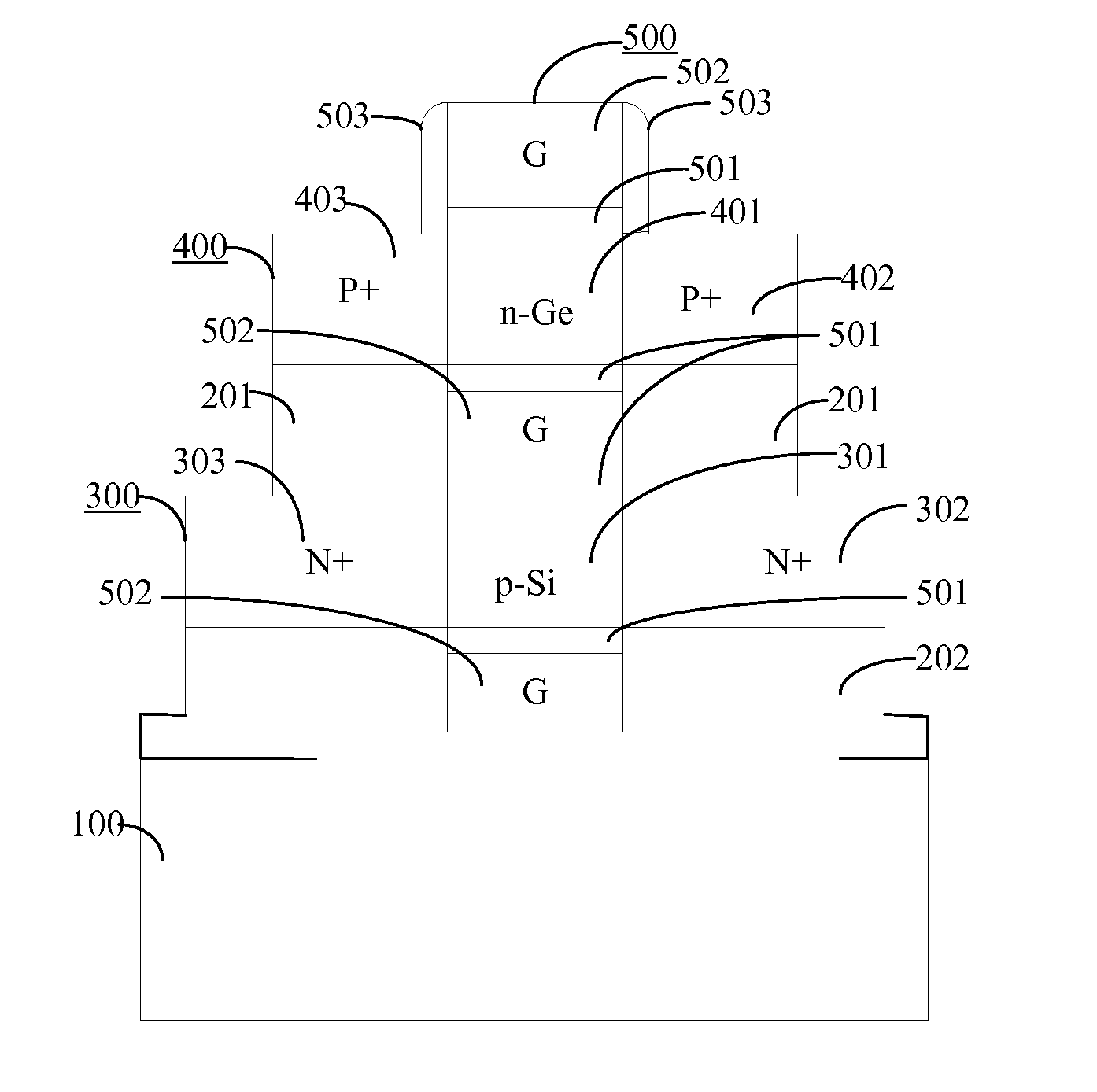
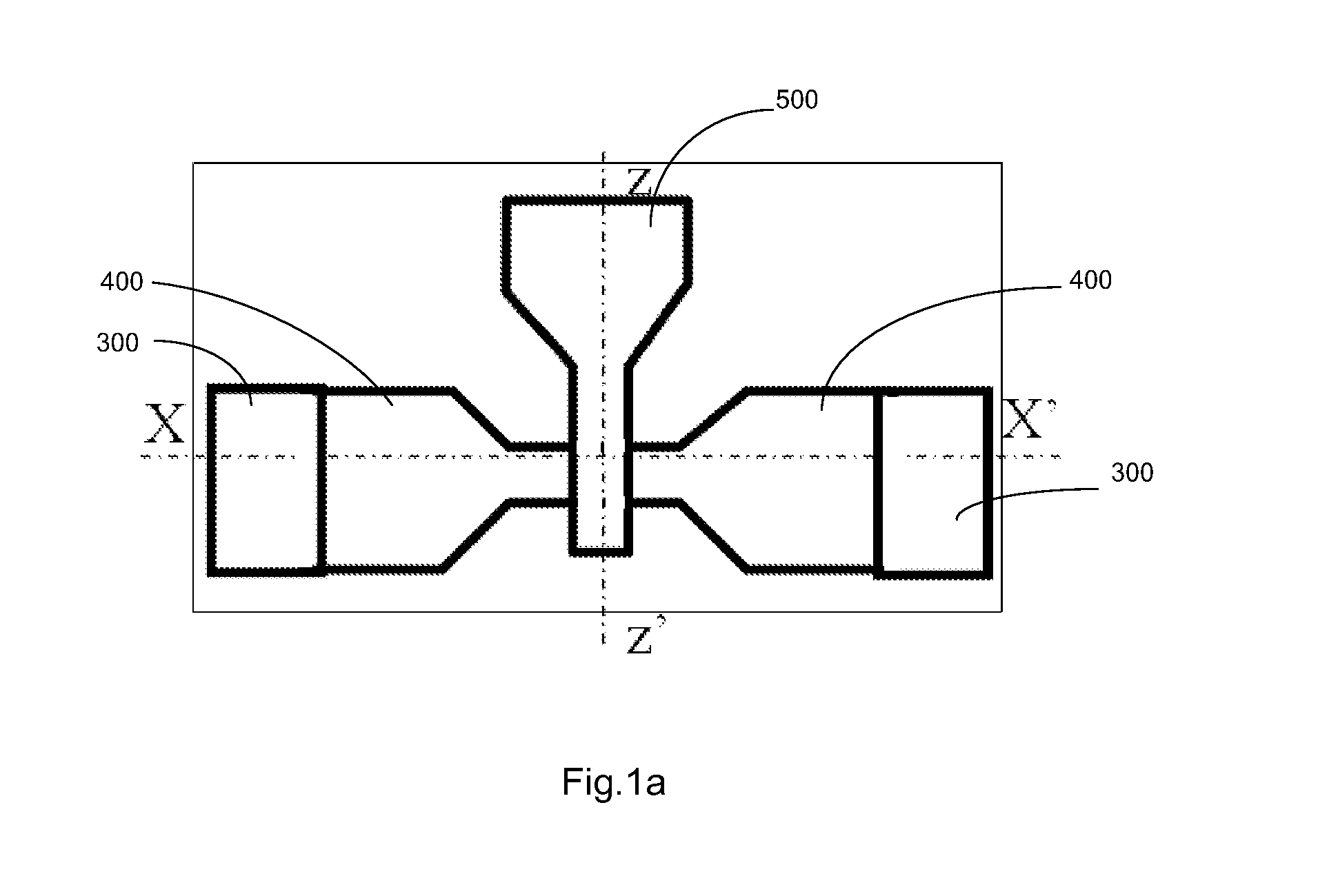
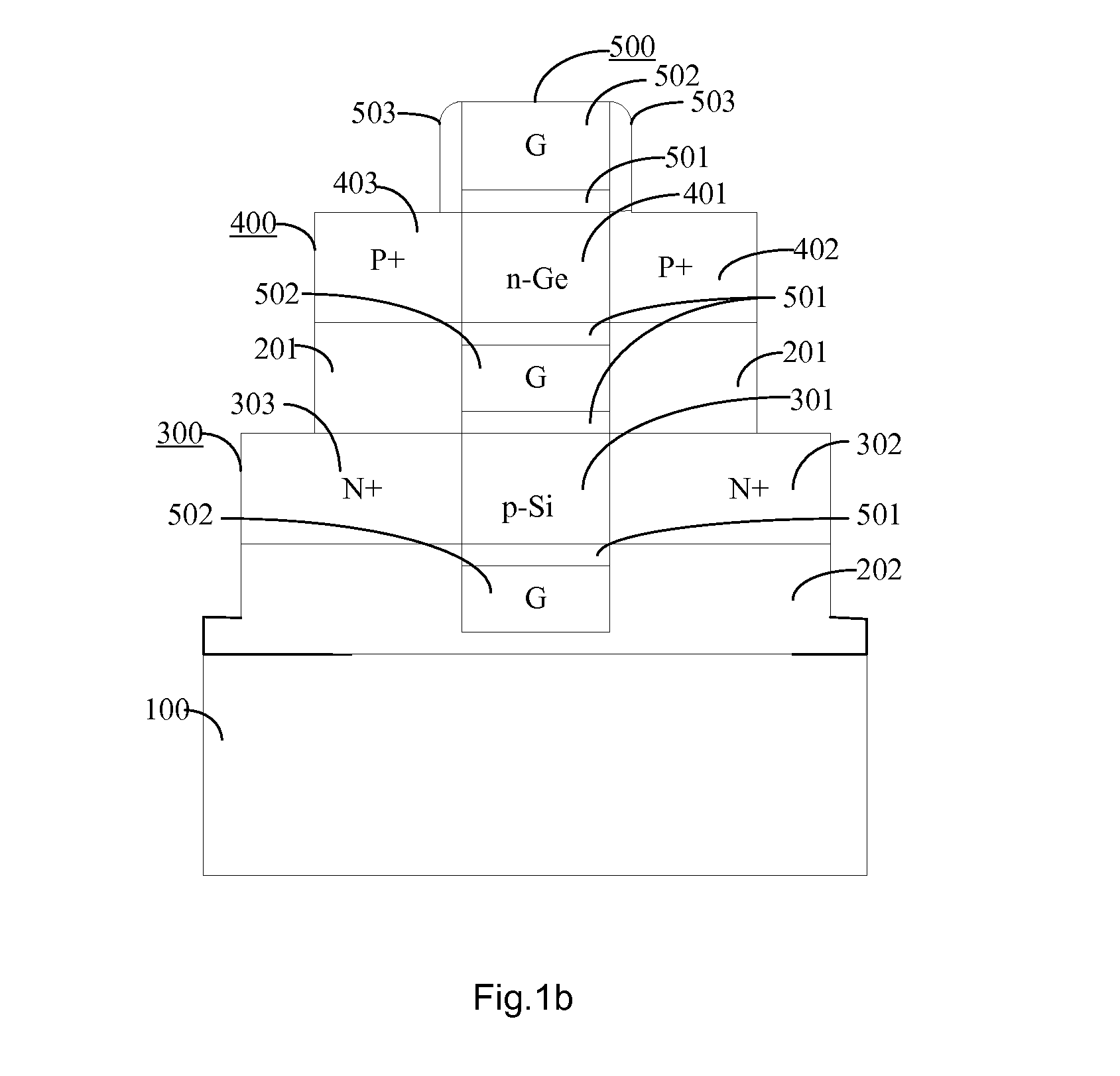
[0019]Referring to FIGS. 1a-1c, a hybrid material inversion mode GAA CMOSFET of the first embodiment includes: a semiconductor substrate 100, a PMOS region 400 having a channel 401, an NMOS region 300 having a channel 301, and a gate region 500. Each of the channels 401, 301 has a circular-shaped cross section. The channel 401 is preferably formed of n-type Ge and the second channel 301 is preferably formed of p-type Si. The gate region 500 substantially surrounds the surfaces of the channels 401, 301.

[0020]In FIG. 1b, a first buried oxide (BOX) layer 201 is disposed between the PMOS region 400 and the NMOS region 300, other than the gate region 500, to avoid inter-region interference. A second buried oxide layer 202 is disposed between the NMOS region 300 and the underlying semiconductor substrate 100 (i.e. Si substrate), other than the gate region 500, to isolate the NMOS region 300 from the underlying semiconductor substrate 100. The BOX layers effectively reduce the leakage curr...

second embodiment

[0025]FIGS. 4a-4c shows another embodiment of the device. The hybrid material inversion mode GAA CMOSFET includes: a semiconductor substrate 100′, a PMOS region 400′ having a channel 401′, an NMOS region 300′ having a channel 301′, and a gate region 500′. The channel 401′ and the channel 301′ each has a circular-shaped cross section, and the channel 401′ is made of a semiconductor material different from the channel 301′. In the present embodiment, the channel 401′ is preferably formed of n-type Ge and the channel 301′ is preferably formed of p-type Si. The gate region 500′ surrounds the surfaces of the channels 401′, 301′. A first buried oxide (BOX) layer 201′ is disposed between the PMOS region 400′ and the NMOS region 300′, other than the gate region 500′, to avoid inter-region interference. A second buried oxide (BOX) layer 202′ is disposed between the PMOS region 400′ and the underlying semiconductor substrate 100′, other than the gate region 500′, to isolate the PMOS region 40...


PUM


Abstract

A Ge and Si hybrid material inversion mode GAA (Gate-All-Around) CMOSFET includes a PMOS region having a first channel, an NMOS region having a second channel and a gate region. The first channel and the second channel have a circular-shaped cross section and are formed of n-type Ge and p-type Si, respectively; the surfaces of the first channel and the second channel are substantially surrounded by the gate region; a buried oxide layer is disposed between the PMOS region and the NMOS region and between the PMOS or NMOS region and the Si substrate to isolate them from one another. In an inversion mode, current flows through the overall cylindrical channel, so as to achieve high carrier mobility, reduce low-frequency noises, prevent polysilicon gate depletion and short channel effects and increase the threshold voltage of the device.

Description

BACKGROUND OF THE INVENTION[0001]1. Technical Field[0002]The present invention relates generally to the field of semiconductor manufacturing technologies and more particularly to a hybrid material inversion mode GAA (Gate-All-Around) CMOSFET (Complementary Metal Oxide Semiconductor Field Effect Transistor).[0003]2. Description of Related Art[0004]A CMOS device integrates both NMOS (N-type Metal Oxide Semiconductor) and PMOS (P-type Metal Oxide Semiconductor) transistors in one device. As the device size continues to shrink, a major challenge in scaling down the channel length is to maintain a high current drive capability (Ion) and a stable threshold voltage, and control the device leakage current (Ioff) at the same time. Short channel effect (SCE) degrades device performance and is a severe obstacle to scale down the channel length.[0005]SOI (Silicon on Insulator) technology uses an ‘engineered’ substrate in place of a conventional bulk silicon substrate. The ‘engineered’ substrate...

Claims


Application Information

Patent Timeline
Patent Type & Authority Applications(United States)
IPC IPC(8): H01L27/092
CPCH01L21/823807H01L21/823821H01L29/42392H01L27/1211H01L21/845
Inventor XIAO, DEYUANWANG, XIZHANG, MIAOCHEN, JINGXUE, ZHONGYING
Owner SHANGHAI INST OF MICROSYSTEM & INFORMATION TECH CHINESE ACAD OF SCI
Why Eureka
Try Eureka