Low voltage low light imager and photodetector

Active Publication Date: 2011-10-20
CALIFORNIA INST OF TECH
View PDF4 Cites 62 Cited by
  • Summary
  • Abstract
  • Description
  • Claims
  • Application Information

AI Technical Summary

Benefits of technology

[0015]The current invention is directed to a highly efficient, compact, low mass imaging photodetector capable of operating as an Electron Bombarded Array (EBA, either CCD or CMOS), Night Vision system, or Image Tube, the inventive photodetector shall be referred to hereinafter as a Della-Doped Electron Bombarded Array (DDEBA), wh

Problems solved by technology

The problem is that silicon sensors are almost never solar blind, a feature that is required for use in most interplanetary applications.
While it is possible to make a camera system solar blind by using optical. filtering, the UV/visible rejection ratio desired by most planetary applications places enormous burdens on the filler designer.
The less than unity UV/visible response-ratio of silicon sensors makes a challenging job even more difficult.
However, realistically, it will be more than a decade before monolithic imagers (not photocathodes) in these new materials can provide performance equivalent to silicon imagers.
While MCP-based imagers have been used successfully, they have significant drawbacks, such as low QE, limited resolution, small format size, limited number of pixels, high voltage requirements, and difficulty of fabrication in sealed-tube configuration.
Also, format size cannot exceed 60 mm without great cost and difficulty, especially in sealed tubes.
There are also practical. difficulties that can make their inclusion in low-cost, short-duration flight development programs problematic (in particular, th

Method used


Image

  • Low voltage low light imager and photodetector
  • Low voltage low light imager and photodetector
  • Low voltage low light imager and photodetector

Examples


Example

Example 1

DDCCD Detector Array

[0116]A versatile thinning approach that can accommodate detectors with various formats and structures and is compatible with die or wafer format has been developed for the production of DDCCD detector arrays in accordance with the current invention. (See, T. J. Jones, et al., Proc. Of SPIE, 3965, January (2000), the disclosure of which is incorporated herein by reference.) FIGS. 13a and b qualitatively shows the specular surface of a thinned packaged delta-doped CCD in accordance with this invention. Surface profilometry has been used to quantify the optical. flatness of the thinned CCD. Nine 10-mm scans were made across the surface of an etched CCD. FIG. 14 shows a 200-μm segment of a line scan, which is typical. of the entire etched surface. The data show a 200 Å peak-to-peak variation in the height of the etch surface. This degree of flatness is suitable for the demanding requirements of optics in space instruments.

Example

Example 2

Proximity Focusing and Visible Light Rejection

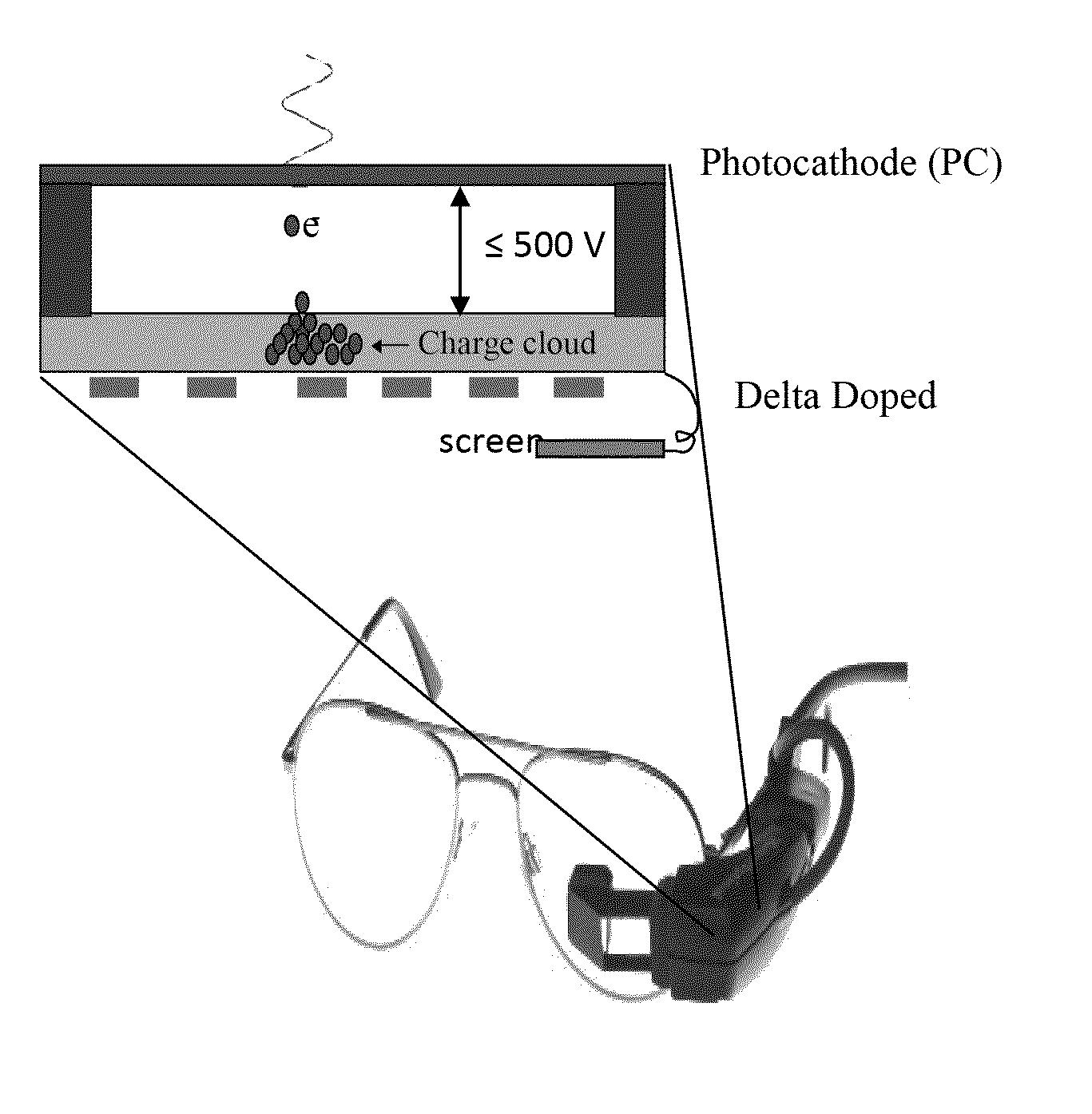
[0117]The large reduction in required electron energies to produce a detectable signal., in accordance with the current invention makes possible a radical. simplification of the conventional. EBCCD architecture. Since lateral photoelectron energies are a few eV, resolutions of 20-30 microns can be achieved with a proximity-focused design in which the semitransparent photocathode is separated from the CMOS or CCD by a few hundred microns and with a 500-1000V potential. The permanent magnet, which is used in conventional. EBCCDs, is deleted in this configuration. Thus a very compact device can be produced as shown in FIGS. 13a and b. However, one issue remains, namely, visible light rejection. In the DDEBA design of the current invention, the photocathode absorbs photons (whether UV or near-IR) producing electrons that are detected in the delta doped APS with a voltage dependent gain (typically 300). At the same time, visible phot...

Example

Example 3

Exemplary Applications

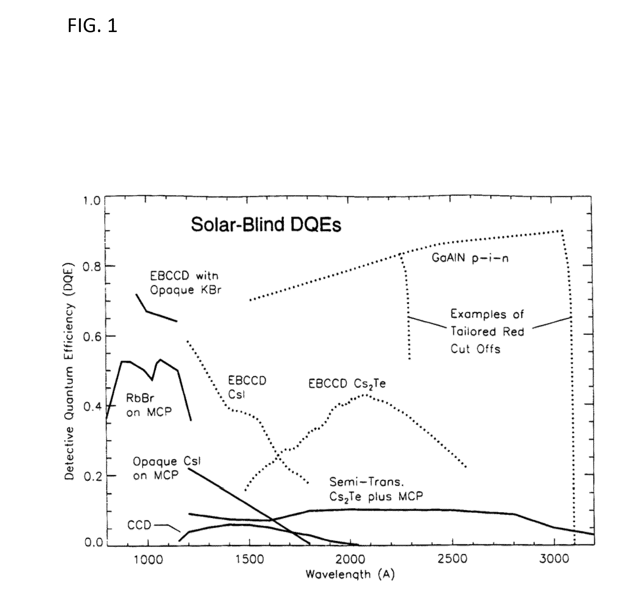
[0121]Examples of science objectives and classes of missions requiring UV / VUV instruments are given below. Traditionally, MCPs have been used for these applications. While these work well, they have limits, and for decades scientists have attempted the development of newer technology solar-blind UV detectors that would operate without high voltage, have low noise background, large pixel. arrays with a uniform response across the array, and not be limited by count rates as MCP detectors are locally and globally. This is now possible through the current invention. DDEBAs will enable miniaturization, simplification, and low-power consumption while improving the performance of UV / VUV instruments.

Atmospheric Detection and Composition Studies

[0122]High efficiency and compact spectrometers and imagers can be mission enabling. VUV observations of the extended upper atmospheres of all of the planets and their satellites are needed, due to the small columns of g...


PUM


Abstract

Highly efficient, low energy, low light level imagers and photodetectors are provided. In particular, a novel class of Della-Doped Electron Bombarded Array (DDEBA) photodetectors that will reduce the size, mass, power, complexity, and cost of conventional imaging systems while improving performance by using a thinned imager that is capable of detecting low-energy electrons, has high gain, and is of low noise.

Description

STATEMENT OF RELATED APPLICATIONS[0001]The current application claims priority to U.S. Provisional. Application No. 61 / 303,558, filed Feb. 11, 2010, the disclosure of which is incorporated herein by reference.STATEMENT AS TO FEDERALLY SPONSORED RESEARCH[0002]The invention described herein was made in the performance of work under a NASA contract, and is subject to the provisions of Public Law 96-517 (35 USC 202) in which the Contractor has elected to retain title.FIELD OF THE INVENTION[0003]The current invention is directed to imagers and photodetectors; and more particularly to low voltage, low light imagers and photodetectors for use as night vision goggles, electron bombarded Charge-Coupled Device (CCD) or Complementary Metal-Oxide-Semiconductor (CMOS) imagers and image tubes.BACKGROUND OF THE INVENTION[0004]Current detection technology can be classified into two major categories: (1) solid-state devices based on silicon or wide bandgap semiconductors, and (2) a combination of ph...

Claims


Application Information

Patent Timeline
IPC IPC(8): H01L31/18H01L27/146
CPCH01L27/14643H01L27/14694H01L27/14806H01L31/0304Y02E10/544H01L31/107H01L31/1844H02N2/18H01L31/03529
Inventor NIKZAD, SHOULEHMARTIN, CHRISHOENK, MICHAEL E.
Owner CALIFORNIA INST OF TECH
Why Eureka
Try Eureka