

Photosensitive imaging devices and associated methods
a technology of imaging devices and associated methods, applied in the direction of radiation controlled devices, optical radiation measurement, instruments, etc., can solve the problems of registration errors, serious problems for applications with high accuracy, and often too dark scenes to discern details
- Summary
- Abstract
- Description
- Claims
- Application Information
AI Technical Summary
Benefits of technology
Problems solved by technology
Method used
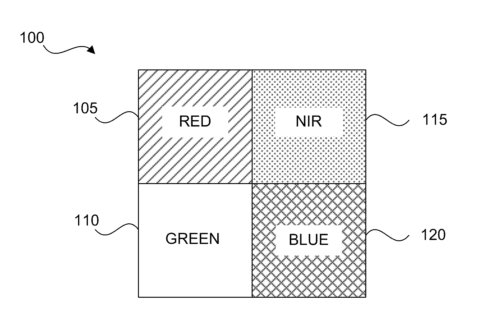
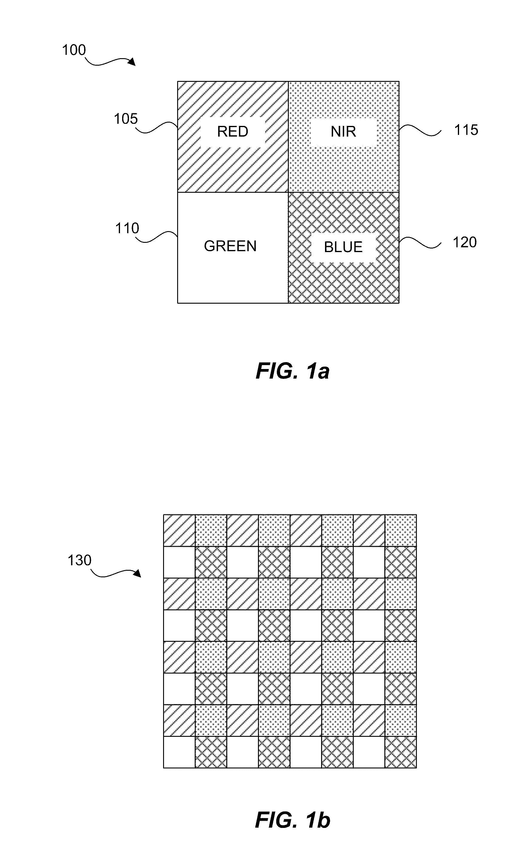
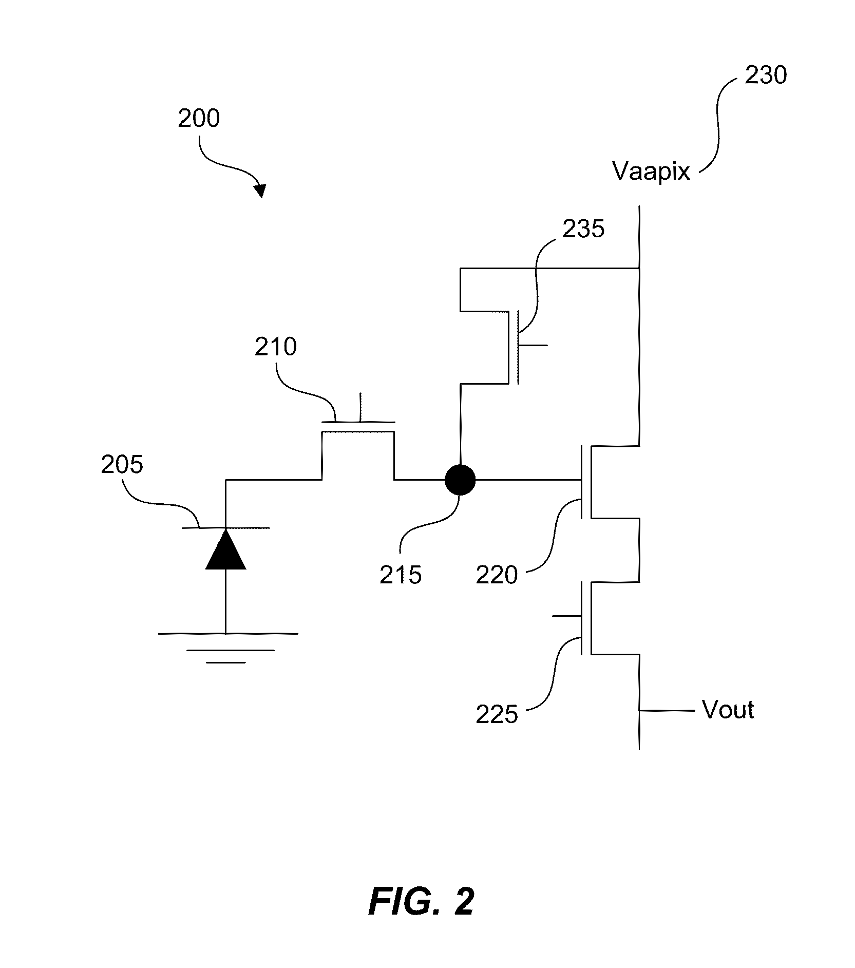
Image

Examples
Embodiment Construction
[0020]Before the present disclosure is described herein, it is to be understood that this disclosure is not limited to the particular structures, process steps, or materials disclosed herein, but is extended to equivalents thereof as would be recognized by those ordinarily skilled in the relevant arts. It should also be understood that terminology employed herein is used for the purpose of describing particular embodiments only and is not intended to be limiting.
[0021]Definitions
[0022]The following terminology will be used in accordance with the definitions set forth below.
[0023]It should be noted that, as used in this specification and the appended claims, the singular forms “a,” and, “the” include plural referents unless the context clearly dictates otherwise. Thus, for example, reference to “a dopant” includes one or more of such dopants and reference to “the layer” includes reference to one or more of such layers.
[0024]As used herein, the terms “light” and “electromagnetic radia...
PUM
 Abstract
Description
Claims
Application Information