Optical semiconductor device and method of manufacturing optical semiconductor device

Active Publication Date: 2011-10-27
SUMITOMO ELECTRIC DEVICE INNOVATIONS
View PDF7 Cites 3 Cited by
  • Summary
  • Abstract
  • Description
  • Claims
  • Application Information

AI Technical Summary

Benefits of technology

[0006]It is effective to narrow a hole leak path, in order to reduce a threshold current of a semiconductor laser. In concrete, two ways of arranging an n-type InP burying layer closer to a p-type cladding layer and reducing a thickness of the p-type cladding layer are effective.

Problems solved by technology

However, it is difficult to make a distance between the n-type InP burying layer and the p-type cladding layer constant in a wafer face, because of temperature distribution in the wafer face and a decomposition rate difference of material gas, and so on.
This may result in variation of a narrowed width.
The mask may cause a distortion of the active layer when the thickness of the p-type cladding layer is reduced.
Accordingly, it is difficult to narrow the hole leak path.

Method used


Image

  • Optical semiconductor device and method of manufacturing optical semiconductor device
  • Optical semiconductor device and method of manufacturing optical semiconductor device
  • Optical semiconductor device and method of manufacturing optical semiconductor device

Examples


first embodiment

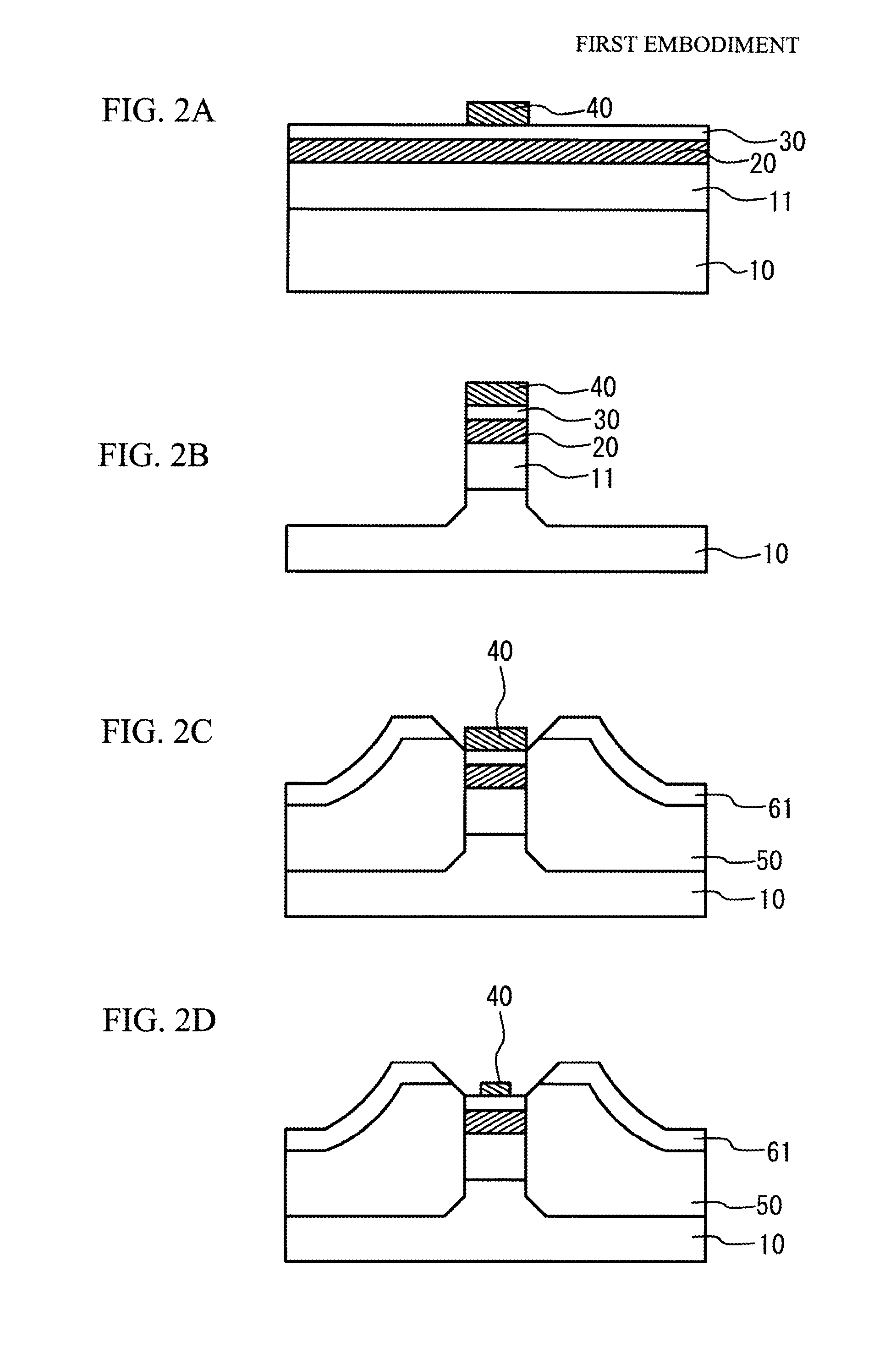
[0027]A description will be given of a method of manufacturing a semiconductor laser in accordance with a first embodiment. FIG. 2A through FIG. 4 illustrate the method of manufacturing the semiconductor laser in accordance with the first embodiment. As illustrated in FIG. 2A, the n-type cladding layer 11, the active layer 20 and the p-type cladding layer 30 are grown on the n-type InP substrate 10. Next, the mask 40 is formed in a stripe shape on an area of the p-type cladding layer 30 where the mesa stripe is to be formed.

[0028]The n-type InP substrate 10 is, for example, made of n-type InP in which Sn (tin) of 1.0×10¹⁸ / cm3 is doped. The n-type cladding layer 11 is, for example, made of n-type InP having a thickness of 0.5 μm in which Si (silicon) of 1.0×10¹⁸ / cm3 is doped. For example, the active layer 20 has an InGaAsP-based multiple quantum well structure. The p-type cladding layer 30 is, for example, made of p-type InP having a thickness of 0.2 μm in which Zn (zinc) of 1.0×10¹⁸...

second embodiment

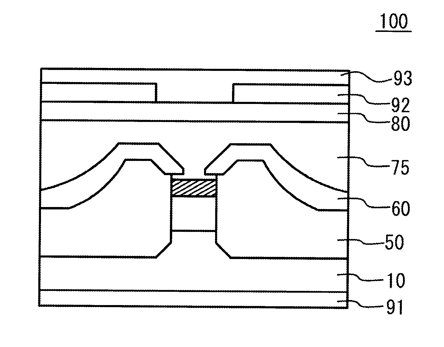
[0041]The first burying layer 50 may have a structure in which a highly resistive semiconductor layer and a p-type semiconductor layer are laminated. FIG. 7A illustrates a schematic cross sectional view of a semiconductor laser 100a in accordance with a second embodiment. The semiconductor laser 100a is different from the semiconductor laser 100 of FIG. 4 in a point that a burying layer in which a highly resistive semiconductor layer 52 is laminated on a p-type semiconductor layer 51 is provided instead of the first burying layer 50. Impurity such as Fe, Ti or Co generating deep acceptor level is doped in the highly resistive semiconductor layer 52. With the structure, an element capacity may be reduced more, compared to a case where a p-type InP is used as the first burying layer 50. Thus, the frequency characteristics of the semiconductor laser 100a are improved.

[0042]FIG. 7B illustrates a method of manufacturing the semiconductor laser 100a. As illustrated in FIG. 7B, instead of ...

third embodiment

[0044]FIG. 8 illustrates a schematic cross sectional view of a semiconductor layer 100b in accordance with a third embodiment. The same components as those illustrated in FIG. 8 have the same reference numerals as FIG. 4. In the embodiment, “W” and “h” of a region between the active layer 20 and the second burying layer 60 are researched. The “h” is a height from the active layer 20 to a lower face of the second burying layer 60 formed in the process of FIG. 3A. The “W” is a width of the depressed face of the second burying layer 60 above the active layer 20.

[0045]Samples 1 to 3 of Table 1 were manufactured having a different combination of “W” and “h”.

TABLE 1HEIGHT hWIDTH W(nm)(nm)W / hSAMPLE 11202001.7SAMPLE 21002002.0SAMPEL 3801602.0

[0046]FIG. 9 illustrates the current characteristics of the samples 1 to 3 of the semiconductor laser 100b. In FIG. 9, a horizontal axis indicates a current provided to the semiconductor lasers, and a vertical axis indicates outputting power of the semi...


PUM


Abstract

A method of manufacturing an optical semiconductor device including: forming a mesa structure including a first conductivity type cladding layer, an active layer and a second conductivity type cladding layer in this order on a first conductivity type semiconductor substrate, an upper most surface of the mesa structure being constituted of an upper face of the second conductivity type cladding layer; growing a first burying layer burying both sides of the mesa structure at higher position than the active layer; forming an depressed face by etching both edges of the upper face of the second conductivity type cladding layer; and growing a second burying layer of the first conductivity type on the depressed face of the second conductivity type cladding layer and the first burying layer.

Description

CROSS-REFERENCE TO RELATED APPLICATION[0001]This application is based upon and claims the benefit of priority of the prior Japanese Patent Application No. 2010-102729, filed on Apr. 27, 2010 and Japanese Patent Application No. 2011-057014, filed on Mar. 15, 2011, the entire contents of which are incorporated herein by reference.BACKGROUND[0002](i) Technical Field[0003]The present invention relates to an optical semiconductor device and a method of manufacturing an optical semiconductor device.[0004](ii) Related Art[0005]Japanese Patent Application Publication No. 2000-174389 discloses a semiconductor laser in which a p-type InP, an n-type InP and a p-type InP bury a mesa stripe including an active layer. The semiconductor laser may be manufactured through a process of burying the mesa stripe by laminating the p-type InP, the n-type InP and the p-type InP after forming the mesa stripe.SUMMARY[0006]It is effective to narrow a hole leak path, in order to reduce a threshold current of a...

Claims


Application Information

Patent Timeline
IPC IPC(8): H01S5/227H01L21/20B82Y40/00
CPCH01L21/02392H01L21/02461H01L21/02543H01L21/02576H01S5/3013H01L21/02581H01S5/2227H01S5/2275H01S5/20H01L21/02579
Inventor TAKEUCHI, TATSUYAHASEGAWA, TARO
Owner SUMITOMO ELECTRIC DEVICE INNOVATIONS
Why Eureka
Try Eureka