Nonvolatile memory device and method for fabricating the same

a memory device and non-volatile technology, applied in the direction of semiconductor devices, basic electric elements, electrical appliances, etc., can solve the problems of increasing the difficulty of fabricating semiconductor devices, the difficulty of satisfying both conditions, and the limitations of fabrication technology, so as to improve the erase operation speed and the retention characteristic

Inactive Publication Date: 2011-11-03
SK HYNIX INC
View PDF4 Cites 196 Cited by
  • Summary
  • Abstract
  • Description
  • Claims
  • Application Information

AI Technical Summary

Benefits of technology

[0010]An exemplary embodiment of the present invention is directed to a semiconductor memory device and a method for fabricating the same, which is capable of improving the erase operation speed and the retention characteristic.

Problems solved by technology

As the integration degree of semiconductor devices rapidly increases, the difficulty in fabricating the semiconductor devices has been increasing, and the fabrication technology has been reaching its limits.
However, since the erase speed and the retention characteristic are in a trade-off relation, there are difficulties for satisfying both conditions.
That is, when silicon is rich, the charge trap or charge storage layer exhibits an excellent erase operation characteristic, but exhibits a poor retention characteristic.
However, when a multilayer is applied, a very thin nitride layer needs to be deposited two-three times. In this case, there are difficulties in forming a nitride layer having a uniform thickness on a hole barrier with a high aspect ratio.
Furthermore, as the deposition temperature of the nitride layer is high, thermal stress increases as much, thereby reducing the reliability of a device.

Method used


Image

  • Nonvolatile memory device and method for fabricating the same
  • Nonvolatile memory device and method for fabricating the same
  • Nonvolatile memory device and method for fabricating the same

Examples


first embodiment

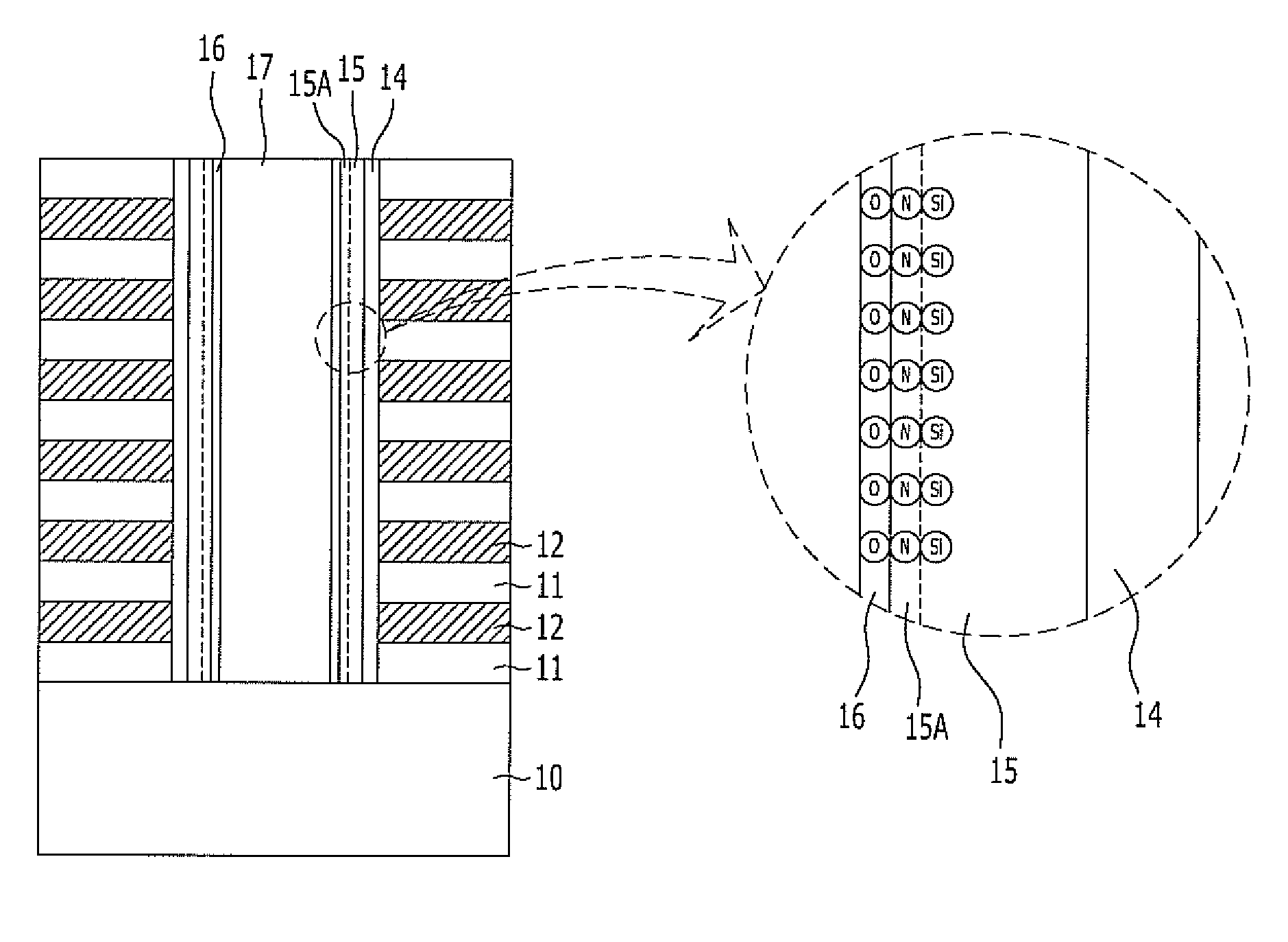
[0025]FIG. 1 is a cross-sectional view illustrating a nonvolatile memory device in accordance with a first embodiment of the present invention.

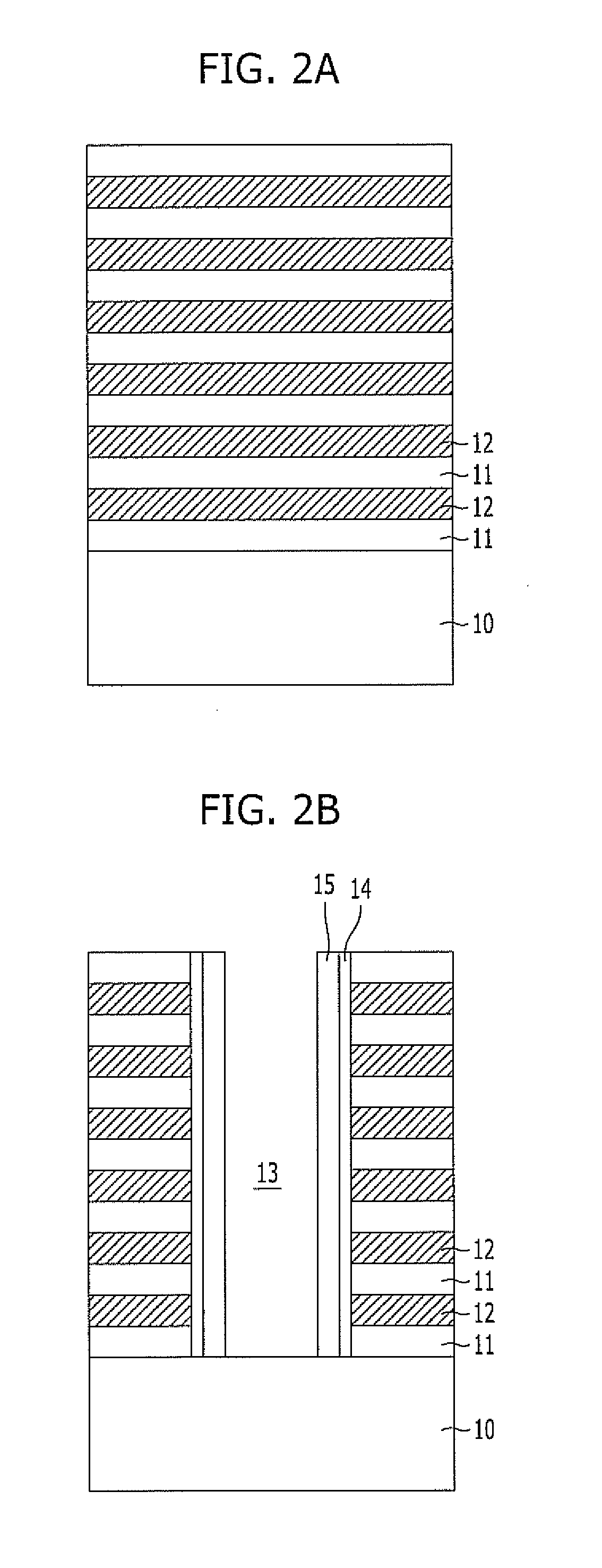
[0026]Referring to FIG. 1, a plurality of interlayer dielectric layers 11 and a plurality of gate electrode conductive layers 12 are alternately stacked on a substrate 10 including desired lower structures such as a source line and a lower selection transistor. Here, the interlayer dielectric layers 11 are provided to isolate a plurality of stacked memory cells from each other, and may be formed of oxide. Furthermore, the gate electrode conductive layers 12 may be formed of polysilicon doped with P-type or N-type impurities.

[0027]Depending on the number of memory cells to be stacked on the substrate 10, the interlayer dielectric layers 11 and the gate electrode conductive layers are repetitively formed. The interlayer dielectric layers 11 and the gate electrode conductive layers 12 may be respectively formed to have a thickness of 100 Å to 80...

second embodiment

[0055]FIG. 3 is a sectional view illustrating a nonvolatile memory device in accordance with a second embodiment of the present invention.

[0056]Referring to FIG. 3, a plurality of interlayer dielectric layers 21 and a plurality of gate electrode conductive layers 22 are alternately stacked on a substrate 20 including desired lower structures such as a source line and a lower selection transistor.

[0057]A cell channel portion which is not illustrated in FIG. 3 is formed passing through the interlayer dielectric layers 21 and the gate electrode conductive layers 22 to expose the substrate 20. A charge blocking layer 24 and a charge trap or charge storage layer 25 are formed on sidewalls of the cell channel portion.

[0058]The charge trap or charge storage layer 25 is used as a substantial data storage place, serves to trap charges in a deep-level trap site, and may be formed of nitride. In particular, the charge trap or charge storage layer 25 may be formed of silicon nitride, for exampl...

third embodiment

[0063]FIG. 4 is a cross-sectional view illustrating a nonvolatile memory device in accordance with a third embodiment of the present invention.

[0064]Referring to FIG. 4, a plurality of interlayer dielectric layers 31 and a plurality of gate electrode conductive layers 32 are alternately stacked on a substrate 30 including desired lower structures such as a source line and a lower selection transistor.

[0065]A cell channel portion which is not illustrated in FIG. 4 is formed passing through the interlayer dielectric layers 31 and the gate electrode conductive layers 32 to expose the substrate 30. A charge blocking layer 34 and a charge trap or charge storage layer 35 are formed on sidewalls of the cell channel portion.

[0066]The charge trap or charge storage layer 35 is used as a substantial data storage place, serves to trap charges in a deep-level trap site, and may be formed of nitride. In particular, the charge trap or charge storage layer 35 may be formed of silicon nitride, for e...


PUM


Abstract

A nonvolatile memory device includes a plurality of interlayer dielectric layers and conductive layers for gate electrodes alternately stacked over a substrate, a channel trench passing through the interlayer dielectric layers and the conductive layers and exposing the substrate, a charge blocking layer and a charge trap or charge storage layer formed on sidewalls of the trench, a coupling prevention layer formed at the surface of the charge trap or charge storage layer, and a tunnel insulation layer formed over the coupling prevention layer.

Description

CROSS-REFERENCE TO RELATED APPLICATIONS[0001]The present application claims priority of Korean Patent Application No. 10-2010-0040171, filed on Apr. 29, 2010, which is incorporated herein by reference in its entirety.BACKGROUND OF THE INVENTION[0002]Exemplary embodiments of the present invention relate to a semiconductor fabrication technology, and more particularly, to a nonvolatile memory device of a vertical-channel type and a method for fabricating the same.[0003]As the integration degree of semiconductor devices rapidly increases, the difficulty in fabricating the semiconductor devices has been increasing, and the fabrication technology has been reaching its limits. In addressing such limitations, technology for vertically forming memory cells by using a multi-stack structure has been proposed.[0004]A nonvolatile memory device having vertical channels basically uses silicon-oxide-nitride-oxide-silicon (SONOS) cells using a charge trap or charge storage layer. However, the SONOS...

Claims


Application Information

Patent Timeline
Patent Type & Authority Applications(United States)
IPC IPC(8): H01L29/792H01L21/28
CPCH01L21/28273H01L27/11578H01L27/11582H01L29/513H01L29/7889H01L29/66666H01L29/66825H01L29/7827H01L29/7926H01L29/518H01L29/40114H10B43/20H10B43/27
Inventor KIM, BEOM-YONGLEE, KI-HONG
Owner SK HYNIX INC
Why Eureka
Try Eureka