Solid state neutron detector

a solid-state neutron and detector technology, applied in the field of neutron detectors, can solve the problems of low false-positive detection capability of neutrons, relatively poor gamma insensitivity, manufacturing and operation risks, etc., and achieve high neutron capture cross section, low cost, and high intrinsic efficiency

Inactive Publication Date: 2011-11-03
TREX ENTERPRISES CORP
View PDF2 Cites 62 Cited by
  • Summary
  • Abstract
  • Description
  • Claims
  • Application Information

AI Technical Summary

Benefits of technology

[0010]This invention provides a low-cost device for the detection of thermal neutrons. Thin layers of a material chosen for high absorption of neutrons with a corresponding release of ionizing particles are stacked in a multi-layer structure interleaved with thin layers of hydrogenated amorphous silicon PIN diodes. Some of the neutrons passing into the stack are absorbed in the neutron absorbing material producing neutron reactions with the release of high energy ionizing particles. These high-energy ionizing particles pass out of the neutron absorbing layers into the PIN diode layers creating electron-hole pairs in the intrinsic (I) layers of the diode layers; the electrons and holes are detected by the PIN diodes. These stacks can be mass-produced at very low cost utilizing integrated circuit fabrication processes. A preferred neutron absorbing material is boron 10 (10B) which has a high neutron capture cross section and splits into a high-energy alpha particle and a high-energy lithium 7 isotope each of which can produce ionization in the hydrogenated amorphous silicon PIN diodes.
[0011]Preferred embodiments utilize boron enriched in the boron-10 (10B) isotope. When a neutron passes through the detector, the interaction of the neutrons with the 10B isotopes generates ionizing alpha particles and lithium 7 particles to produce electron hole pairs in the intrinsic layers of the PIN diodes. Preferred embodiments include 5, 10, 15 and 22 layer stacks. The stacked structure can provide very high intrinsic efficiency (greater than 80% for a twenty-two 10B layer stack) for thermal neutron detection.
[0012]The multiple diodes are electrically combined in parallel to provide the total neutron-induced signal current thus enabling a low overall bias voltage (≈10 V) for the detector. The a-Si:H diodes have a very low cross section for gamma radiation and discrimination circuitry is used to further reduce detection of incident gamma rays. Fast neutrons (with energies greater than 1 eV) can be detected by enclosing the thermal neutron detector in a neutron moderator material (polyethylene, for example) that slows the fast neutrons to thermal velocities.
[0013]A key element of invention is the use of hydrogenated amorphous silicon (a-Si:H) for the interleaved diodes. The disordered structure of a-Si:H provides an elastic property to the semiconductor material, relative to crystalline semiconductor materials. This elastic property enables the stacking of a plurality of 10B layers interleaved with the a-Si:H diodes by reducing the interfacial stress between layers. In addition, the a-Si:H diodes can be deposited directly onto metal electrode substrate material. Several other isotopes are available that produce high-energy ionizing particles with the absorption of neutrons and can be used in the place of the boron-10 isotope.

Problems solved by technology

Neutron detectors are used for monitoring of cargo containers and vehicles for nuclear weapons because neutrons are emitted by radiological materials of interest such as plutonium and they are difficult to shield.
These detectors are also relatively insensitive to high energy electromagnetic (gamma) radiation thus enabling very low false positive detection capability for neutrons.
10BF3 proportional tubes come in similar sizes as the 3He tubes, but typically have ⅕ the sensitivity of the 3He tubes and relatively poor gamma insensitivity.
The 10BF3 gas is toxic and each neutron reaction produces three fluorine atoms that are highly corrosive; this poses manufacturing and operational risks for this technology.
However, crystalline semiconductor neutron detectors cannot be stacked to provide higher neutron detection efficiency.
The relatively high cost of these technologies has resulted in limited deployment.

Method used


Image

  • Solid state neutron detector
  • Solid state neutron detector
  • Solid state neutron detector

Examples


first preferred embodiment

Five 10B Layer Neutron Detector

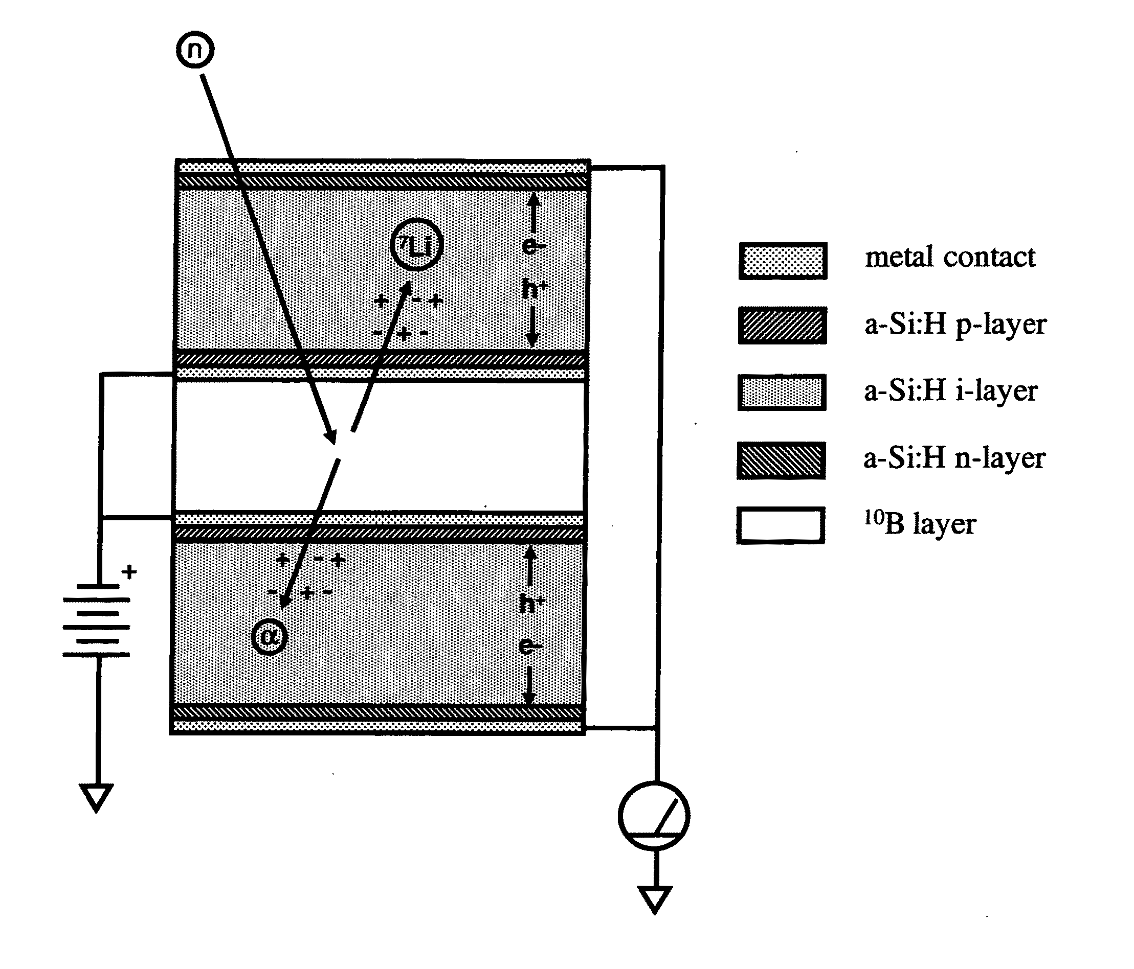
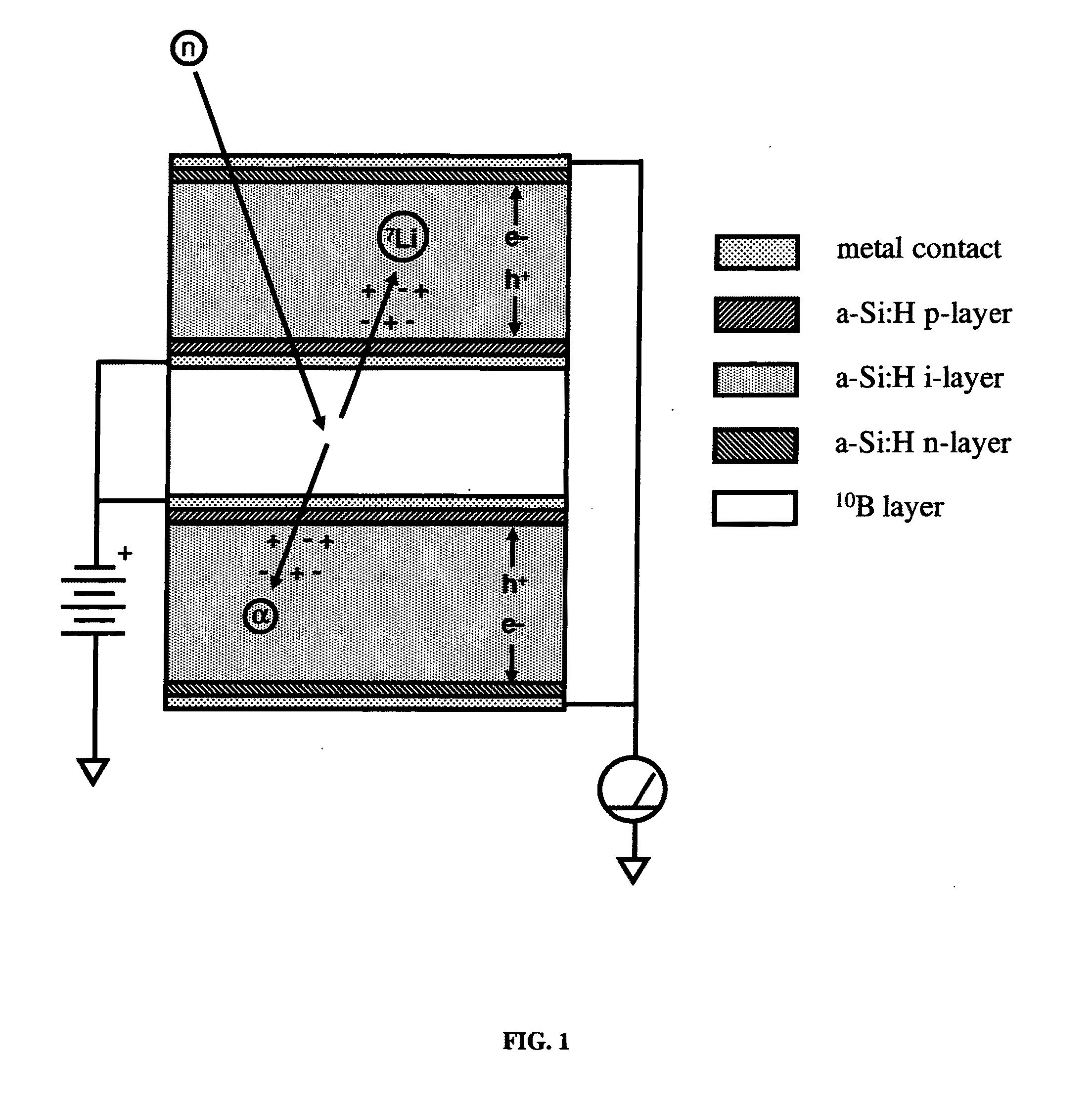
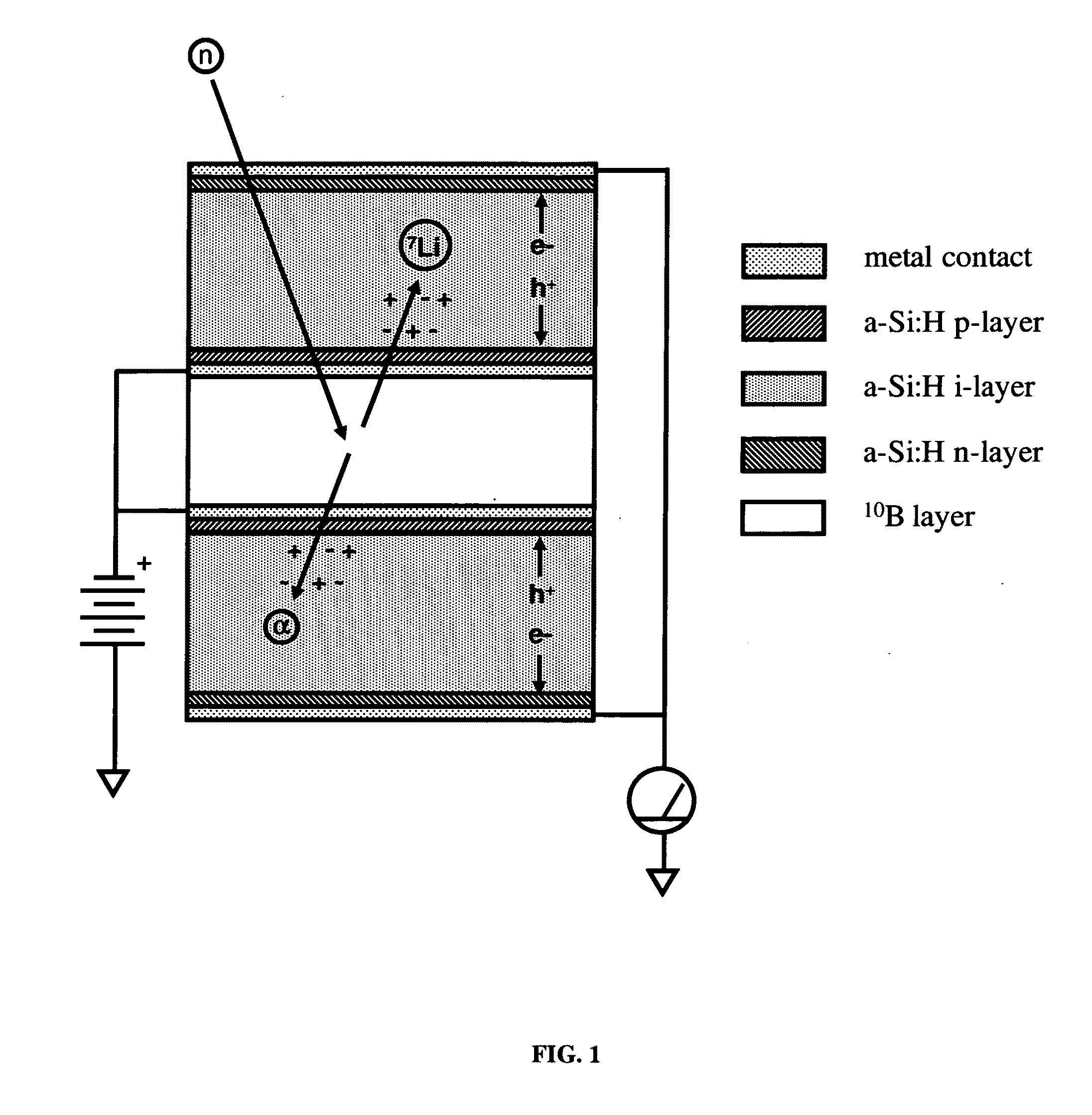
[0034]FIG. 5 shows a cross-sectional diagram of the preferred embodiment of the invention involving five 10B layers interleaved between six hydrogenated amorphous silicon (a-Si:H) PIN diodes. As a single neutron passes through the detector, it will have an eight percent probability of being absorbed in the first 10B layer, assuming a 1.6 micron thick layer of greater than 90% enriched 10B in the 10B layers. If the first 10B layer (N=1) does not absorb the neutron, then the other 10B layers (N=2, 3, 4, 5) will contribute to the total intrinsic efficiency PABS(N=5) according to the equation

[0035]PABS(N)=1−exp└−NPABS,SINGLELAYER┘

where PABS,SINGLELAYER=0.08 is the intrinsic efficiency for neutron detection in a single 10B layer device. FIG. 6 shows a graph of the intrinsic efficiency for detecting neutrons PABS (N) versus number of 10B layers N. FIG. 6 shows that the preferred embodiment has PABS(N=5)=34% intrinsic efficiency for detecting neutrons.

[0036]F...


PUM


Abstract

A low-cost device for the detection of thermal neutrons. Thin layers of a material chosen for high absorption of neutrons with a corresponding release of ionizing particles are stacked in a multi-layer structure interleaved with thin layers of hydrogenated amorphous silicon PIN diodes. Some of the neutrons passing into the stack are absorbed in the neutron absorbing material producing neutron reactions with the release of high energy ionizing particles. These high-energy ionizing particles pass out of the neutron absorbing layers into the PIN diode layers creating electron-hole pairs in the intrinsic (I) layers of the diode layers; the electrons and holes are detected by the PIN diodes.

Description

CROSS REFERENCE TO RELATED APPLICATIONS[0001]This application claims the benefit of Provisional Patent Application Ser. No. 61 / 343,488 filed Apr. 28, 2010.FIELD OF THE INVENTION[0002]This invention relates to neutron detectors and in particular to solid state neutron detectors.BACKGROUND OF THE INVENTION[0003]Neutron detectors are used for monitoring of cargo containers and vehicles for nuclear weapons because neutrons are emitted by radiological materials of interest such as plutonium and they are difficult to shield. Neutron detectors are also used in other applications such as medical diagnostics, oil and gas exploration; and scientific research. The prior art includes several different types of neutron detectors, as described here.Helium-3 Tube Detectors[0004]Helium-3 (3He) tube detectors are the dominant technology used for neutron detection due to their superior sensitivity to neutrons. These detectors are also relatively insensitive to high energy electromagnetic (gamma) radi...

Claims


Application Information

Patent Timeline
Patent Type & Authority Applications(United States)
IPC IPC(8): H01L31/117
CPCG01T3/08H01L31/117H01L31/1055
Inventor ENGELMANN, MICHAEL G.MARTIN, PETER
Owner TREX ENTERPRISES CORP
Why Eureka
Try Eureka