Oxide nitride stack for backside reflector of solar cell

a solar cell and oxide nitride technology, applied in the direction of semiconductor devices, electrical equipment, nanotechnology, etc., can solve the problems of reducing affecting the efficiency of solar cells in converting incident light energy into electrical energy, and recombination ra

Inactive Publication Date: 2011-11-10
APPLIED MATERIALS INC
View PDF0 Cites 27 Cited by
  • Summary
  • Abstract
  • Description
  • Claims
  • Application Information

AI Technical Summary

Benefits of technology

[0010]In light of the above, embodiments of the invention generally provide methods for forming a multilayer rear surface passivation layer on a solar cell substrate. The method includes forming a silicon oxide sub-layer having a net charge density of less than or equal to 2.1×10¹¹ Coulombs/cm2 on a rear surface of a p-type doped region formed in a substrate comprising semiconductor material, the rear surface opposite a light receiving surface of the substrate and forming a silicon nitride sub-layer on the silicon oxide sub-layer.
[0011]Embodiments of the invention also include a solar cell device that may be manufactured according methods disclosed herein. The solar cell device includes a substrate comprising a semiconductor material where the substrate has a...

Problems solved by technology

The efficiency at which a solar cell converts incident light energy into electrical energy is adversely affected by a number of factors, including the fraction of incident light that is reflected off the light receiving surface of a solar cell and/or not reflected off the rear surface of a solar cell, and absorbed in the cell structure, such as a passivation layer, and the recombination rate of electrons and holes in a solar cell.
Each time an electron-hole pair recombines, charge carriers are eliminated, thereby reducing the efficiency of the solar cell.
Moreover, the efficiency of the solar cell may be reduced due to a reduction in the carrier lifetime ...

Method used


Image

  • Oxide nitride stack for backside reflector of solar cell
  • Oxide nitride stack for backside reflector of solar cell
  • Oxide nitride stack for backside reflector of solar cell

Examples


example

Example 1

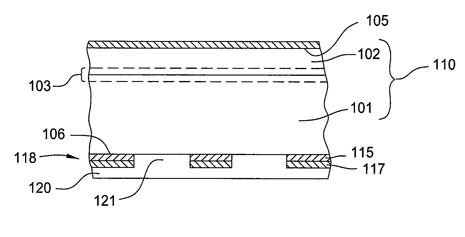
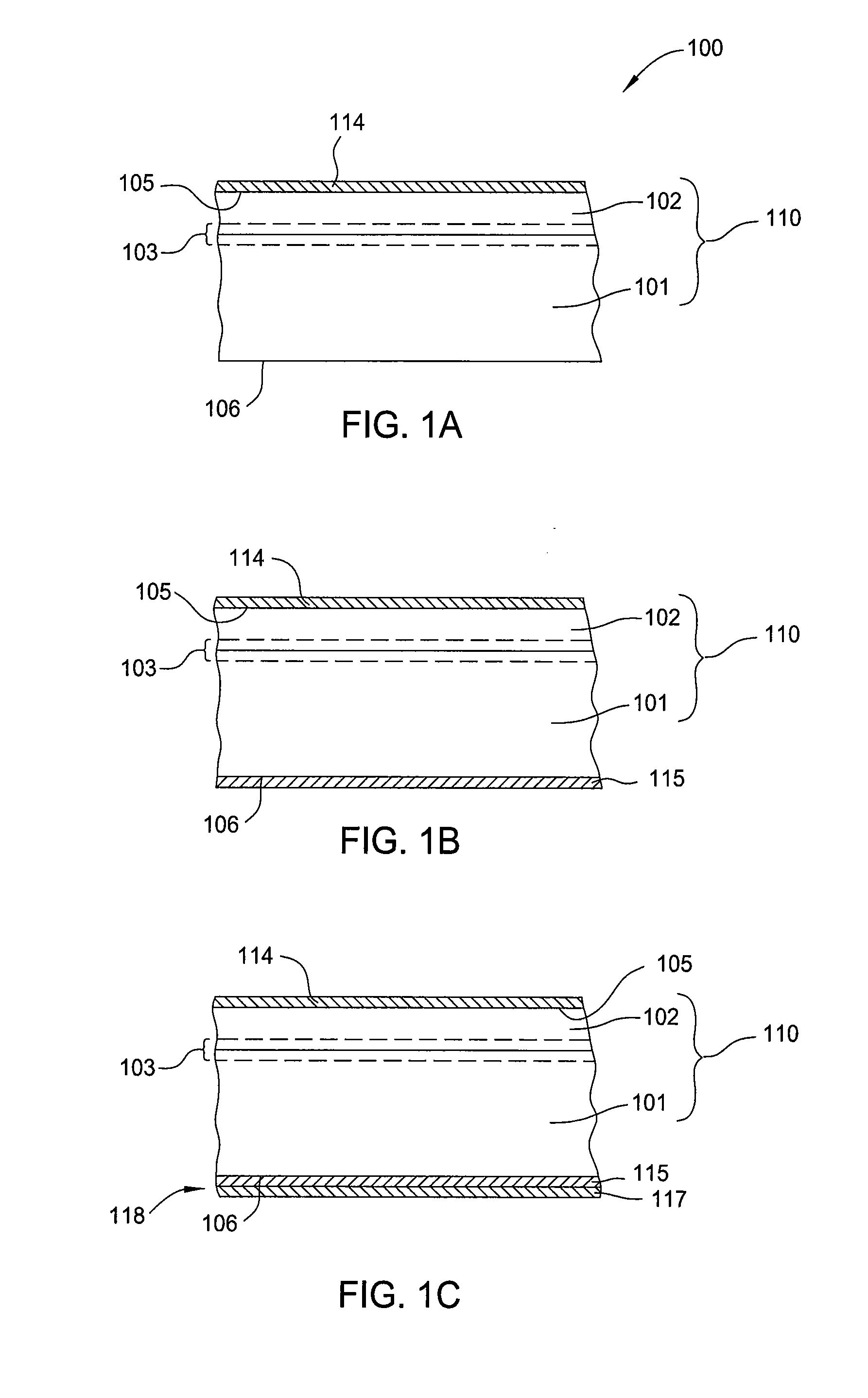
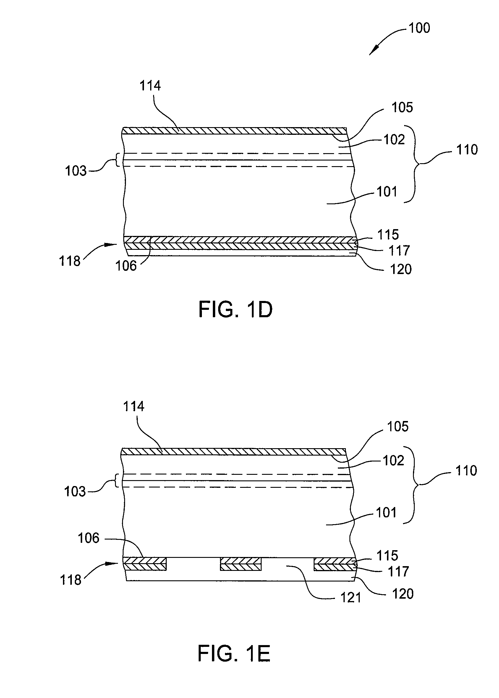
[0068]A silicon oxide sub-layer is deposited on a rear surface of a p-type doped region of a substrate for a solar cell device. A silicon nitride sub-layer is then formed over the silicon oxide sub-layer, thereby forming a multilayer rear surface passivation layer on a solar cell substrate. The silicon oxide and silicon nitride sub-layer are formed according to the following conditions shown in Table 1, and are for a substrate area of 1,200×1,300 mm, which may be used to carry up to 56 wafers in a 7×8 arrangement.

TABLE 1Silicon OxideSilicon NitrideSub-LayerSub-LayerDeposition Time (Sec.)1518Temperature (° C.)390390Pressure (Torr)1.21.5RF Power (Watts)5,50010,000Spacing (mils)1,2001,100N2O flow rate (sccm)15,000N / AN2 flow rate (sccm)N / A17,300TEOS flow rate (sccm)2,0002,000

[0069]The spacing is between the showerhead and the substrate support. The deposition rate for the silicon oxide sub-layer was 3,000 Å per minute and had a thickness of 750 Å. The deposition rate for the si...


PUM


Abstract

Embodiments of the invention generally provide methods for forming a multilayer rear surface passivation layer on a solar cell substrate. The method includes forming a silicon oxide sub-layer having a net charge density of less than or equal to 2.1×10¹¹ Coulombs/cm2 on a rear surface of a p-type doped region formed in a substrate comprising semiconductor material, the rear surface opposite a light receiving surface of the substrate and forming a silicon nitride sub-layer on the silicon oxide sub-layer. Embodiments of the invention also include a solar cell device that may be manufactured according methods disclosed herein.

Description

CROSS-REFERENCE TO RELATED APPLICATIONS[0001]This application claims benefit of U.S. Provisional Patent Application Ser. No. 61 / 332,554 (APPM / 014741 L), filed May 7, 2010, which is herein incorporated by reference.BACKGROUND OF THE INVENTION[0002]1. Field of the Invention[0003]Embodiments of the present invention generally relate to the fabrication of solar cells and particularly to the rear surface passivation of silicon solar cells.[0004]2. Description of the Related Art[0005]Solar cells are photovoltaic devices that convert sunlight directly into electrical power. The most common solar cell material is silicon (Si), which is in the form of single, polycrystalline, multi-crystalline substrates, or amorphous films. Efforts to reduce the cost of manufacturing solar cells, and thus the cost of the resulting cell, while maintaining or increasing the overall efficiency of the solar cell produced are ongoing.[0006]The efficiency of a solar cell may be enhanced by use of a passivation la...

Claims


Application Information

Patent Timeline
IPC IPC(8): H01L31/02H01L31/18B82Y40/00B82Y99/00
CPCH01L31/02168H01L31/056Y02E10/52
Inventor MUNGEKAR, HEMANT P.AGRAWAL, MUKULSTEWART, MICHAEL P.WEIDMAN, TIMOTHY W.MISHRA, ROHITPAAK, SUNHOM
Owner APPLIED MATERIALS INC
Why Eureka
Try Eureka