Laterally Varying II-VI Alloys and Uses Thereof

a technology of iivi alloy and iivi, which is applied in the direction of non-metal conductors, conductors, semiconductor lasers, etc., can solve the problems of limited lattice constant mismatch, large mismatch of materials, and severe limitations in the method of achieving wavelength variability

Active Publication Date: 2011-11-10
ARIZONA STATE UNIVERSITY
View PDF1 Cites 22 Cited by
  • Summary
  • Abstract
  • Description
  • Claims
  • Application Information

AI Technical Summary

Benefits of technology

[0015]In another aspect, the invention provides ZnxCd1-xSySe1-y nanowires wherein x and y are each greater than or equal to 0 and less than or equal to 1.
[0016]In another aspect, the invention provides methods for preparing ZnxCd1-xSySe1-y nanowires comprising contacting at least a portion of a surface of a...

Problems solved by technology

Unfortunately, this method of achieving wavelength variability is severely limited by existing methods of growing planar epitaxial heterostructures of semiconductor thin films on a crystalline substrate.
The very limited lattice constant mismatch required for growing high quality wafers has been the main obstacle of making semiconductor-based optoelectronic devices (such as lasers, detectors, multi-color detectors and solar cells) with controllable and widely variable (or tunable) operating wavelengths.
For epitaxial ...

Method used


Image

  • Laterally Varying II-VI Alloys and Uses Thereof
  • Laterally Varying II-VI Alloys and Uses Thereof
  • Laterally Varying II-VI Alloys and Uses Thereof

Examples


example 1

Growth of CdSxSe1-x Alloy Nanowires

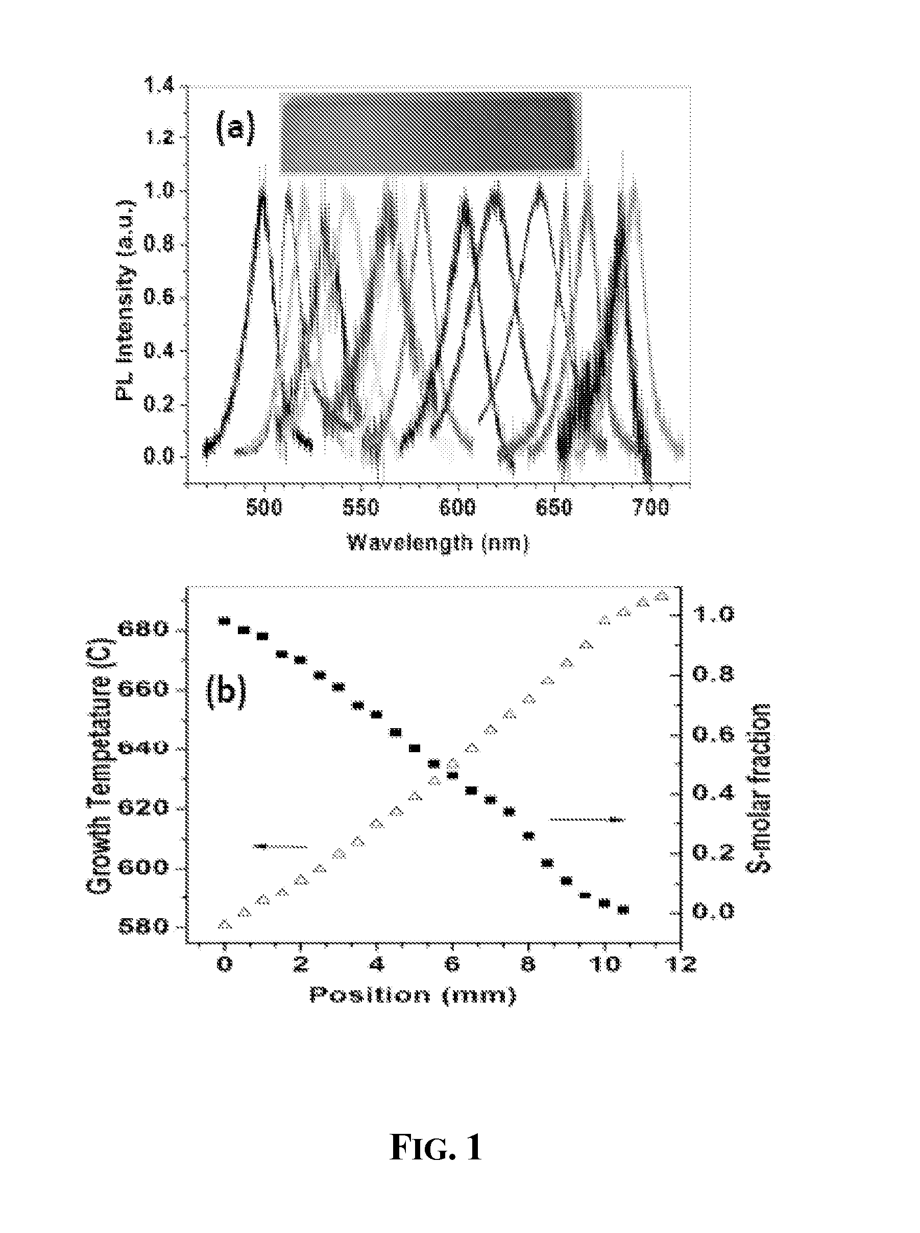
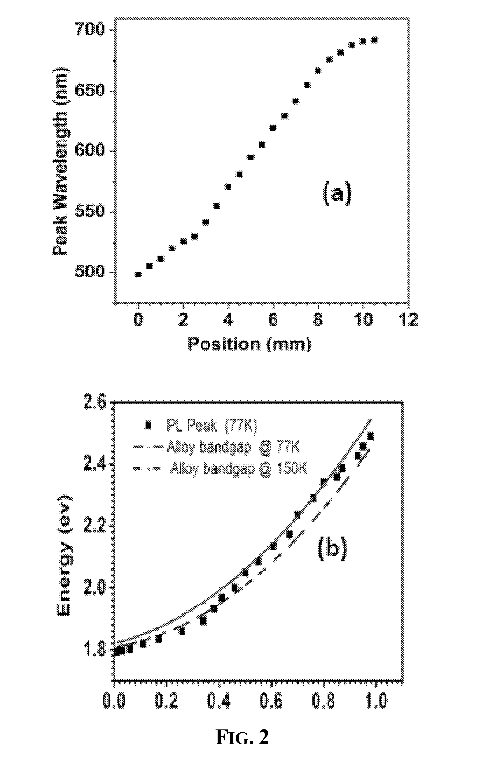
[0132]To demonstrate such widely-spatially-tunable lasing, we chose the ternary alloy CdSxSe1-x (CdSSe) in the full composition range between CdS (x=1, bandgap 2.44 eV) and CdSe (x=0, bandgap 1.72 eV), because they are two important compound semiconductors that are of great interest for their emission in the visible wavelength range and have been investigated for their 1D nanostructures and alloys recently (see, Pan et al., J. Am. Chem. Soc. 127, 15692-1569 (2005); Pan et al., Nanotech. 17, 1083-1086 (2006); Agarwal et al., Nano Lett. 5, 917-920 (2005); Yu et al., J. Am. Chem. Soc. 125, 16168-16169 (2003); Barrelet et al., Nano Lett. 4, 1981-1985 (2004); Ma et al., Nano Lett. 7, 3300-3304 (2007)). For example, CdSSe alloy nanowires with several compositions were grown by changing the ratio of the source powders (CdS and CdSe) and / or the growth temperature of the substrate (see, Pan, 2005, supra; and Pan, 2006, supra). To grow CdSSe nanowires in the...

example 2

Layer Characterization

[0134]1. Photoluminescence: The lasing characteristics of the CdSSe sample of Example 1 was studied using a pulsed (6 ns, 10 Hz), frequency-quadrupled Nd:YAG laser (Spectra Physics Quanta Ray, at 266 nm) as the pump source. The pump beam was focused by a 250 mm focal length lens to a spot size of about 300 μm on the sample at an incidence angle of about 43°. Luminescence from the sample was then collected by a Mitutoyo Objective lens (Plan APO, SL, 50×), placed normal to the sample. The collected light was directed to a 0.3 m spectrometer and detected with a liquid nitrogen cooled CCD detector. The spatial resolution and spectral resolution were estimated to be about 700 nm and 0.2 nm, respectively. For the low temperature measurement, the sample was placed in a microscope cryostat. Liquid nitrogen was used to cool the samples to 77 K. For both the room-temperature and the low-temperature measurements, the sample was scanned across the length of the substrate t...

example 3

Device Integration

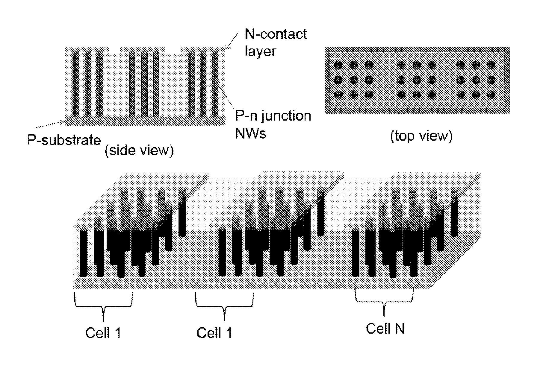
[0139]The substrate of Example 1 can be integrated with electrical contacts according to at least the following methods, for example, to yield structures suitable for use as solar cells. A first integration method is illustrated in FIG. 7a. A catalyst is patterned to provide a lateral array of minicells (Cell 1, Cell 2 . . . Cell N) on the surface of an insulating substrate. The substrate can have dimensions, for example, of about 2-5 mm×20 mm or larger, where the minicells are laterally arranged along the long dimension (20 mm) of the substrate. The extent of each minicell can be selected to yield a given bandgap interval for each minicell. Nanowires can be deposited on the patterned insulating substrate according to the methods of Example 1, where the nanowires deposit on the portions of the substrate having a surface catalyst layer. In FIG. 7a, the mean bandgap of each minicell continuously increases from Cell 1 through Cell N (i.e., left to right). Finally, an ...


PUM


Abstract

Described herein are semiconductor structures comprising laterally varying II-VI alloy layer formed over a surface of a substrate. Further, methods are provided for preparing laterally varying II-VI alloy layers over at least a portion of a surface of a substrate comprising contacting at least a portion of a surface of a substrate within a reaction zone with a chemical vapor under suitable reaction conditions to form a laterally varying II-VI alloy layer over the portion of the surface of the substrate, wherein the chemical vapor is generated by heating at least two II-VI binary compounds; and the reaction zone has a temperature gradient of at least 50-100° C. along an extent of the reaction zone. Also described here are devices such as lasers, light emitting diodes, detectors, or solar cells that can use such semiconductor structures. In the case of lasers, spatially varying wavelength can be realized while in the case of solar cells and detectors multiple solar cells can be achieved laterally where each cell absorbs solar energy of a given wavelength range such that entire solar spectrum can be covered by the said solar cell structure. For LED applications, spatial variation of alloy composition can be used to engineer colors of light emission.

Description

CROSS-REFERENCE TO RELATED APPLICATIONS[0001]This application claims the benefit of the filing date of U.S. Provisional Application Ser. No. 61 / 112,144, filed Nov. 6, 2008, which is hereby incorporated by reference in its entirety.STATEMENT OF GOVERNMENT FUNDING[0002]The invention described herein was made in part with government support under grant number W911NF-08-1-0471, awarded by US Army Research Office. The United States Government has certain rights in the invention.FIELD OF THE INVENTION[0003]The invention generally relates to semiconductor structures comprising laterally varying II-VI alloys, methods for their preparation, and uses thereof. Examples of such uses include, but are not limited to, spatially wavelength varying lasers and light emitting diodes, multi-color detectors and laterally distributed solar cells where each cell absorbs one given wavelength range of solar radiation.BACKGROUND OF THE INVENTION[0004]Alloying two semiconductors of different bandgaps generall...

Claims


Application Information

Patent Timeline
IPC IPC(8): H01L29/221H01B1/10H01L29/225H01L21/40B82Y40/00B82Y99/00
CPCH01L21/02422H01L21/02491H01L2924/0002H01L21/02557H01L21/0256H01L21/02562H01L21/02568H01L21/0262H01L21/02636H01L31/0296H01L31/0352H01L33/02H01L33/28H01S5/1042H01S5/327H01L2924/00
Inventor NING, CUN-ZHENGPAN, ANLIAN
Owner ARIZONA STATE UNIVERSITY
Why Eureka
Try Eureka