Semiconductor laser apparatus, method of manufacturing semiconductor laser apparatus and optical apparatus

a laser apparatus and semiconductor technology, applied in the direction of lasers, semiconductor lasers, solid-state devices, etc., can solve the problems of disadvantageous deterioration of semiconductor laser chips and disadvantageous complex manufacturing process, and achieve the effects of convenient use, easy application, and easy bonding

Inactive Publication Date: 2011-11-17
SANYO ELECTRIC CO LTD
View PDF0 Cites 33 Cited by
  • Summary
  • Abstract
  • Description
  • Claims
  • Application Information

AI Technical Summary

Benefits of technology

[0030]As hereinabove described, the method of manufacturing a semiconductor laser apparatus according to the second aspect of the present invention comprises the step of bonding at least the two of the base portion, the sealing member and the window member to each other through the sealant made of the ethylene-polyvinyl alcohol copolymer by thermocompression bonding. In the present invention, a material, handling of which is easy in a manufacturing process, is employed as the sealant, and hence the package can be sealed by bonding the base portion, the sealing member and the window member to each other without requiring a complicated manufacturing process. Further, the ethylene-polyvinyl alcohol copolymer is employed as the sealant, and hence the semiconductor laser apparatus having the semiconductor laser chip inhibited from deterioration can be obtained.
[0031]In the aforementioned method of manufacturing a semiconductor laser apparatus according to the second aspect of the present invention, the step of bonding preferably includes a step of press-bonding the sealing member and at least one of the base port

Problems solved by technology

Consequently, the semiconductor laser chip is disadvantageously deteriorated.
In the optical module (semiconductor apparatus) disclosed in Japanese Patent Laying-Open No. 2009-135347, the package and the substrate are bonded to e

Method used


Image

  • Semiconductor laser apparatus, method of manufacturing semiconductor laser apparatus and optical apparatus
  • Semiconductor laser apparatus, method of manufacturing semiconductor laser apparatus and optical apparatus
  • Semiconductor laser apparatus, method of manufacturing semiconductor laser apparatus and optical apparatus

Examples


first embodiment

Modification of First Embodiment

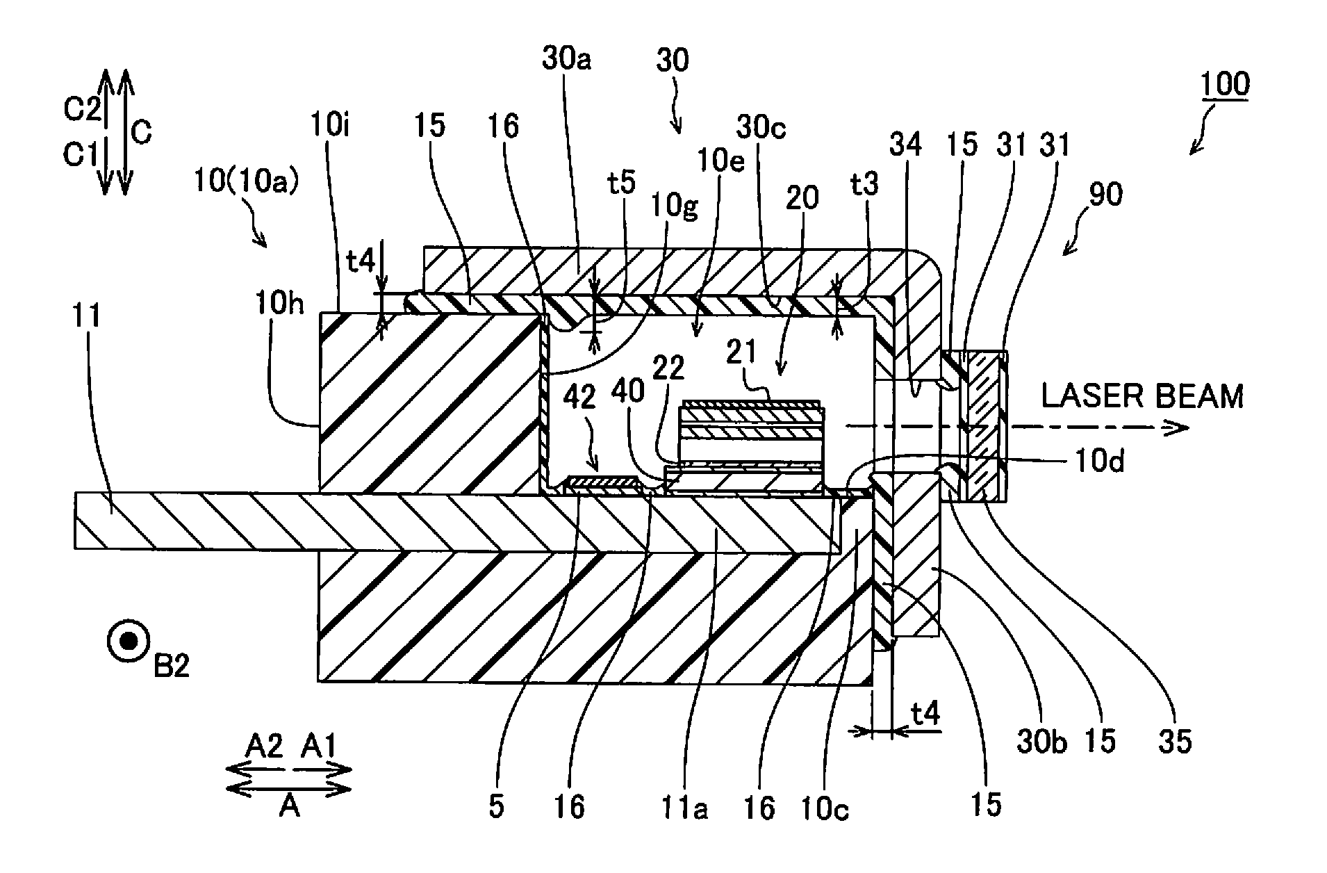
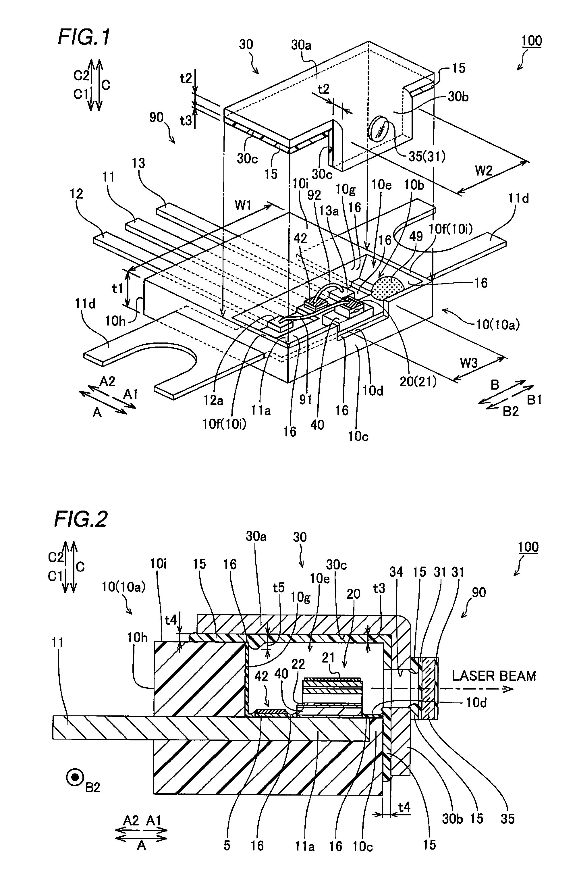
[0104]A semiconductor laser apparatus 105 according to a modification of the first embodiment is now described. In this semiconductor laser apparatus 105, a sealing member 30 is made of aluminum foil with a thickness of about 50 μm. At this time, a sealant 15 is not applied onto an inner surface 30c of the sealing member 30 located in sealed space of a package 90, and a surface of the aluminum foil is exposed in the sealed space. On the other hand, the sealant 15 is applied with a prescribed thickness onto a peripheral region (a region near an inner wall portion 10g and respective upper surfaces of a pair of side wall portions 10f and a front wall portion 10c) of an opening 10e in an upper surface 10i of a base body 10a and a peripheral region of an opening 10d in the front surface (an outer surface (on an A1 side) of the front wall portion 10c) so as to surround the peripheries of the openings 10e and 10d shown in FIG. 1. In this state, the sealing m...

second embodiment

[0108]A semiconductor laser apparatus 200 according to a second embodiment of the present invention is now described. In this semiconductor laser apparatus 200, as shown in FIGS. 9 and 10, a package 90 has a base portion 10, and a sealing member 45 and a window member 46 both mounted on the base portion 10, covering a blue-violet semiconductor laser chip 20 from upper (a C2 side) and front (an A1 side) sides, respectively. While a gas absorbent 49 (see FIG. 1) is not provided in a recess portion 10b in the semiconductor laser apparatus 200, the gas absorbent 49 may be provided in the recess portion 10b.

[0109]A base body 10a has a tapered outer shape in which a width (in a direction B) is decreased toward a front end portion 210c from the back (direction A2) as viewed from a side of an upper surface 10i.

[0110]The sealing member 45 is made of Cu alloy foil such as nickel silver with a thickness t6 of about 15 μm. The sealing member 45 has a planar shape substantially identical to a ...

third embodiment

Modification of Third Embodiment

[0136]A semiconductor laser apparatus 305 according to a modification of the third embodiment is now described. This semiconductor laser apparatus 305 comprises a base portion 315 prepared by forming a recess portion 315b in a substantially rectangular flat metal plate by press working, as shown in FIG. 15. FIG. 16 includes a sectional view showing a mounting structure of a lead frame 12 (13) and the base portion 315 in a part of a longitudinal sectional view taken along the center line of the semiconductor laser apparatus 305 in a width direction (direction B).

[0137]The recess portion 315b is constituted by four side wall portions 316, 317, 318 and 319 surrounding the periphery of the blue-violet semiconductor laser chip 20 and an inner bottom surface 310c for mounting a submount 40. The recess portion 315b has an opening 315e, which opens in an upper surface 10i of the base portion 315. The base portion 315 is provided with a frame-shaped mounting p...


PUM


Abstract

This semiconductor laser apparatus includes a semiconductor laser chip and a package sealing the semiconductor laser chip. The package has a base portion mounted with the semiconductor laser chip, a sealing member and a window member. The semiconductor laser chip is sealed with the base portion, the sealing member and the window member. At least two of the base portion, the sealing member and the window member are bonded to each other through a sealant made of an ethylene-polyvinyl alcohol copolymer.

Description

CROSS-REFERENCE TO RELATED APPLICATION[0001]The priority application numbers JP2010-112231, Semiconductor Laser Apparatus and Optical Apparatus, May 14, 2010, Nobuhiko Hayashi, JP2010-123965, Semiconductor Laser Apparatus and Optical Apparatus, May 31, 2010, Hideki Yoshikawa et al., JP2010-175647, Semiconductor Laser Apparatus, Method of Manufacturing Semiconductor Laser Apparatus and Optical Apparatus, Aug. 4, 2010, Nobuhiko Hayashi et al., and JP2011-041230, Semiconductor Laser Apparatus, Method of Manufacturing Semiconductor Laser Apparatus and Optical Apparatus, Feb. 28, 2011, Nobuhiko Hayashi et al., upon which this patent application is based are hereby incorporated by reference.BACKGROUND OF THE INVENTION[0002]1. Field of the Invention[0003]The present invention relates to a semiconductor laser apparatus, a method of manufacturing a semiconductor laser apparatus and an optical apparatus, and more particularly, it relates to a semiconductor laser apparatus comprising a package...

Claims


Application Information

Patent Timeline
IPC IPC(8): H01S5/022H01L21/52H01S5/0232
CPCH01S5/02212H01S5/02216H01S5/0222H01S5/02228H01S5/02244H01S5/02292H01L2224/48091H01S5/02296H01S5/02469H01S5/0683H01L2924/00014H01L2224/49107H01L2224/73265H01L2924/16195H01S5/02234H01S5/02255H01S5/02257H01S5/0232
Inventor HAYASHI, NOBUHIKOYOSHIKAWA, HIDEKIKURAMOTO, KEIICHINOMURA, YASUHIKOGOTO, TAKENORIOKAYAMA, YOSHIOTOKUNAGA, SEIICHI
Owner SANYO ELECTRIC CO LTD
Why Eureka
Try Eureka