Semiconductor device having ESD structure

Inactive Publication Date: 2011-12-01
LONGITUDE LICENSING LTD
View PDF7 Cites 20 Cited by
  • Summary
  • Abstract
  • Description
  • Claims
  • Application Information

AI Technical Summary

Benefits of technology

[0036]According to an embodiment of the present invention, a phenomenon of which the junction depth of an elevated source/drain region of a peripheral circuit transistor is deeper in the end portion of the active area can be prevented by which a semiconductor layer is epitaxially grown also from the substrate surface exposed when only the STI in the peripheral circuit region is drawn back. Particula

Problems solved by technology

In case of forming high density impurity diffusion layer, a problem of short channel effect is caused due to diffusion of impurities towards a channel.
There is a tendency that as the cell size decreases, a contact size and junction depth decrease, so that it is difficult to secure an electrical characteristic of a device, particularly to make the contact resistance

Method used


Image

  • Semiconductor device having ESD structure
  • Semiconductor device having ESD structure
  • Semiconductor device having ESD structure

Examples


Example

[0045]The invention will be now described herein with reference to illustrative embodiments. Those skilled in the art will recognize that many alternative embodiments can be accomplished using the teachings of the present invention and that the invention is not limited to the embodiments illustrated for explanatory purpose.

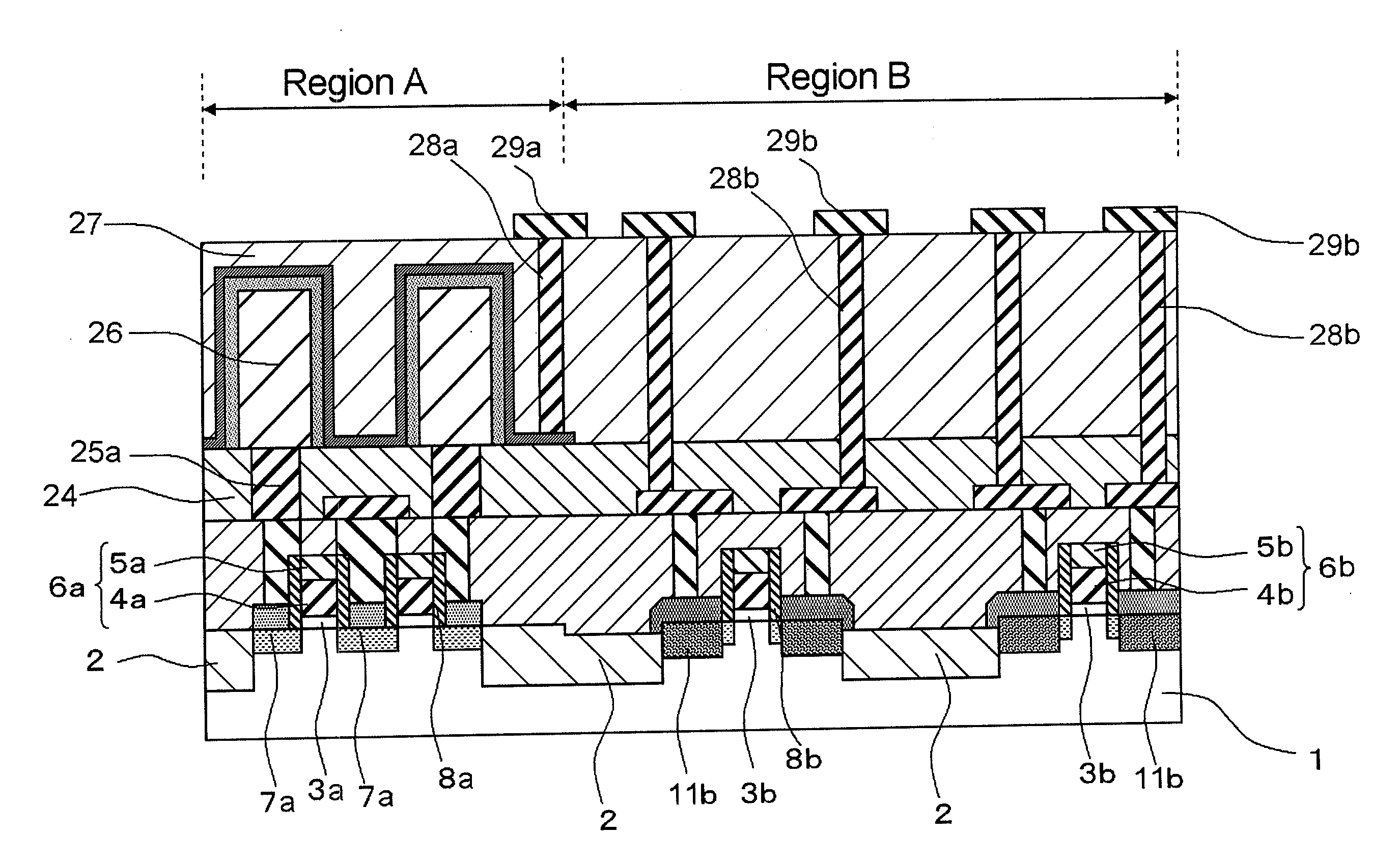
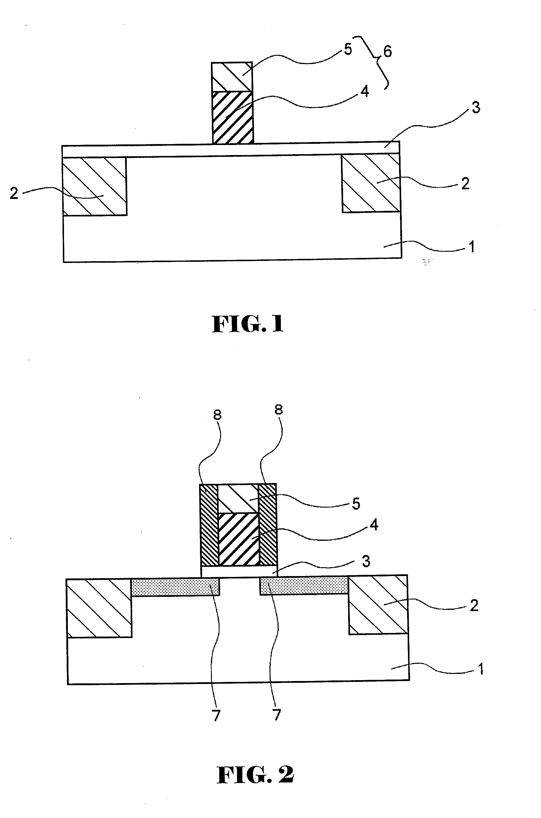
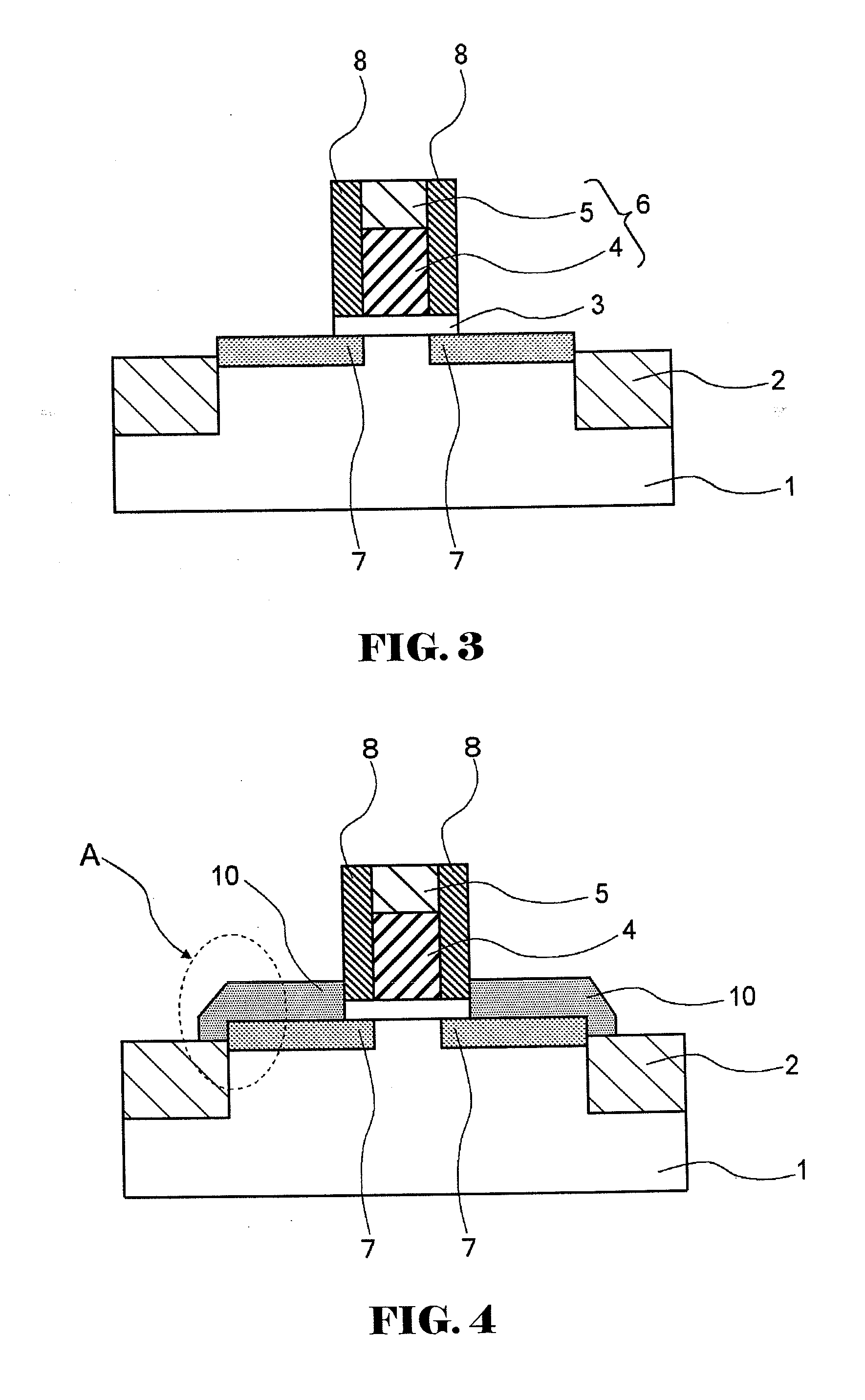
[0046]A description will now be made of the case of forming an N-channel type MOS transistor as an ESD structure peripheral circuit transistor formed in a peripheral circuit region, with reference to the drawings.

(FIG. 1)

[0047]Shallow trench isolation (STI) 2 in which a silicon oxide layer is embedded is formed in semiconductor substrate 1 by means of a conventional STI formation method or the like, thereby defining active areas. Gate insulating layer 3 is formed on semiconductor substrate 1, and a stacked body comprising gate conductive material 4 and cap layer 5 is patterned to form a gate electrode. As gate conductive material 4, a layer of which a metal such a...


PUM


Abstract

Semiconductor layers on active areas for transistors in a memory cell region (region A) and a peripheral circuit region (region B) are simultaneously epitaxially grown in the same thickness in which the adjacent semiconductor layers in region A do not come into contact with each other. Only semiconductor layer (10) in region B is also grown from the surface of a substrate which is exposed when only the surface of STI (2) in region B is drawn back, so that a facet (F) of the semiconductor layer 10 is formed outside the active area, followed by ion-implantation to form a high density diffusion layer (11) in region B. Accordingly, short circuit between semiconductor layers on source/drain electrodes of transistors in region A is prevented, and uniformity of the junction depth of the layer (11) of the source/drain electrodes including an ESD region in a transistor of region B is obtained, thereby restricting the short channel effect.

Description

BACKGROUND OF THE INVENTION[0001]1. Field of the Invention[0002]The present invention relates, in general, to a semiconductor device and, more particularly, to a semiconductor device such as a dynamic random access memory (DRAM) including a transistor having an elevated source / drain (ESD) structure in at least a peripheral circuit region.[0003]2. Description of the Related Art[0004]In a semiconductor device, two or more transistors with different characteristics are often mounted on a single substrate.[0005]For example, a semiconductor device such as a DRAM includes, on a semiconductor substrate, a cell transistor connected to a memory device such as a capacitor, a transistor of an array circuit such as X and Y decoders for control of a memory cell, a transistor of a peripheral circuit for control of data I / O or an array circuit. Generally, from the viewpoint of providing a prescribed area of a memory cell region with cells as many as possible, transistors are closely packed rather ...

Claims


Application Information

Patent Timeline
IPC IPC(8): H01L27/108H01L27/105
CPCH01L27/10873H01L27/10897H01L29/66628H01L27/10894H10B12/05H10B12/09H10B12/50
Inventor IWASA, SHINYA
Owner LONGITUDE LICENSING LTD
Why Eureka
Try Eureka