
High density butted junction CMOS inverter, and making and layout of same

a cmos inverter, high density technology, applied in the direction of basic electric elements, electrical apparatus, semiconductor devices, etc., can solve the problems of compromising device performance and fet becoming more susceptible to short channel effects, and achieve the effect of high circuit density and density of circuitry

Inactive Publication Date: 2011-12-01
IBM CORP
View PDF23 Cites 7 Cited by
  • Summary
  • Abstract
  • Description
  • Claims
  • Application Information

AI Technical Summary

Benefits of technology

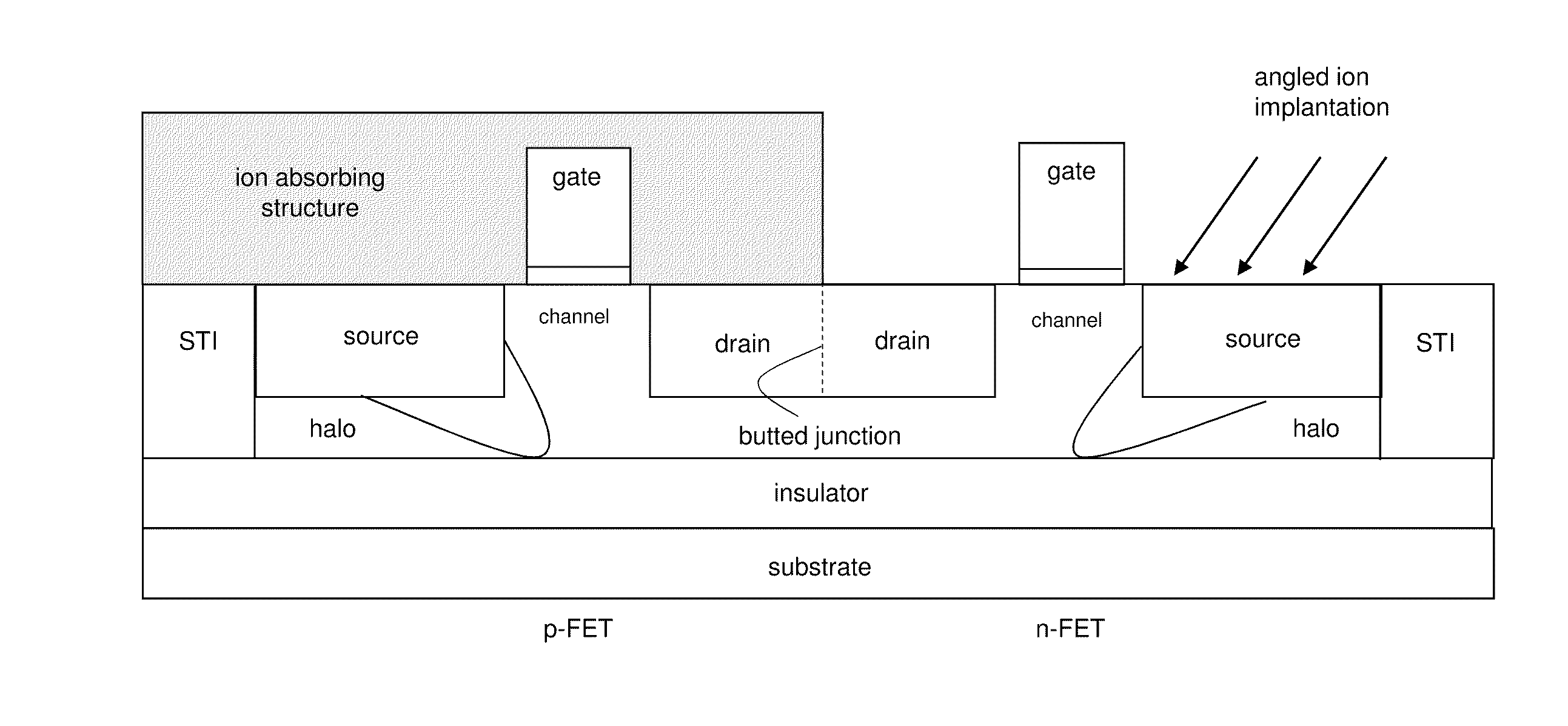
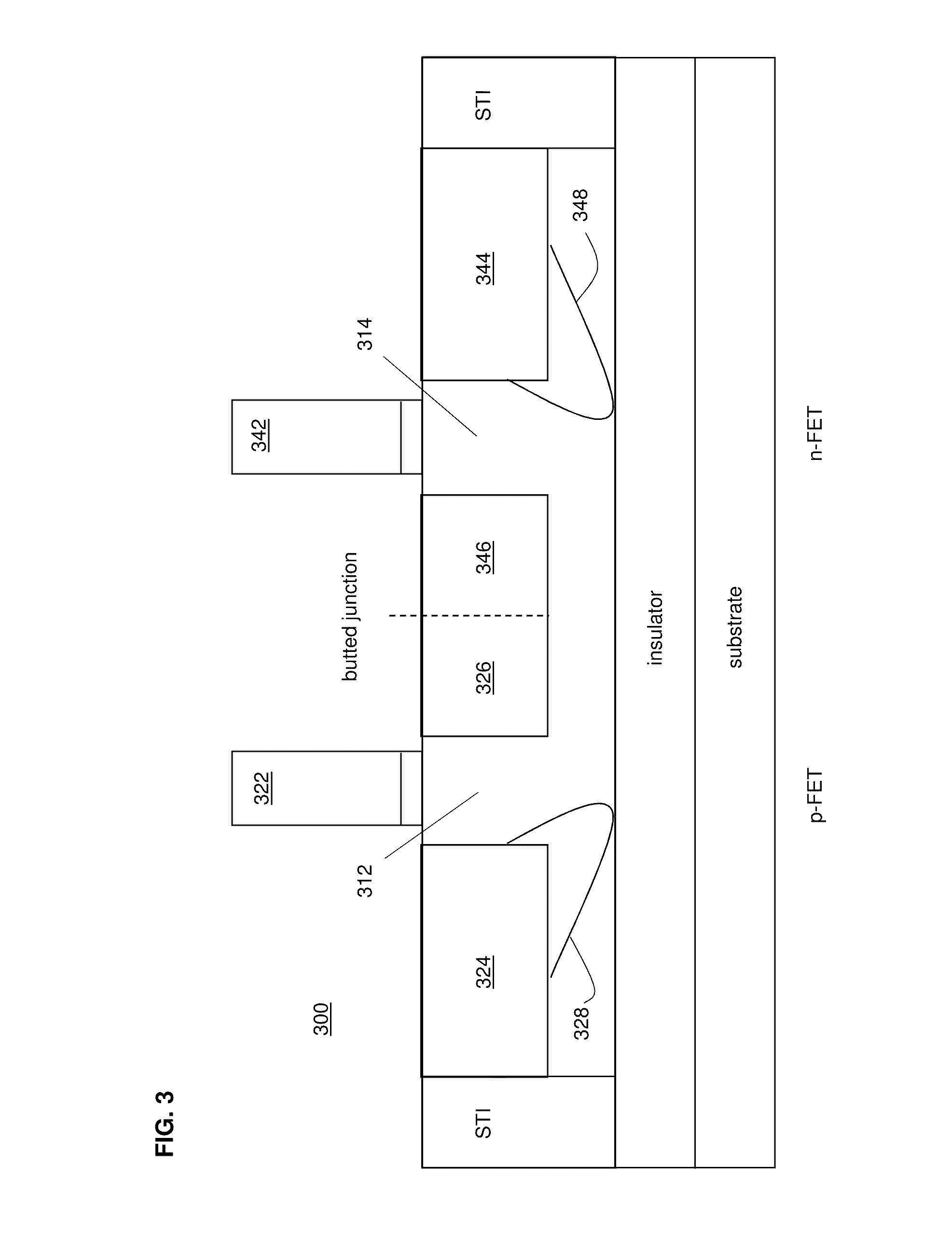
[0015]An aspect of an embodiment of the invention provides for a high circuit density, when the circuitry of an SOI CMOS IC includes a CMOS inverter including an asymmetric p-FET, an asymmetric n-FET, and a butted junction. The density of the circuitry using the asymmetric butted junction CMOS inverter of an exemplary embodiment of the invention is further increased by forming drain regions of the asymmetric p-FET and asymmetric n-FET, which are shorter than their corresponding source regions.

Problems solved by technology

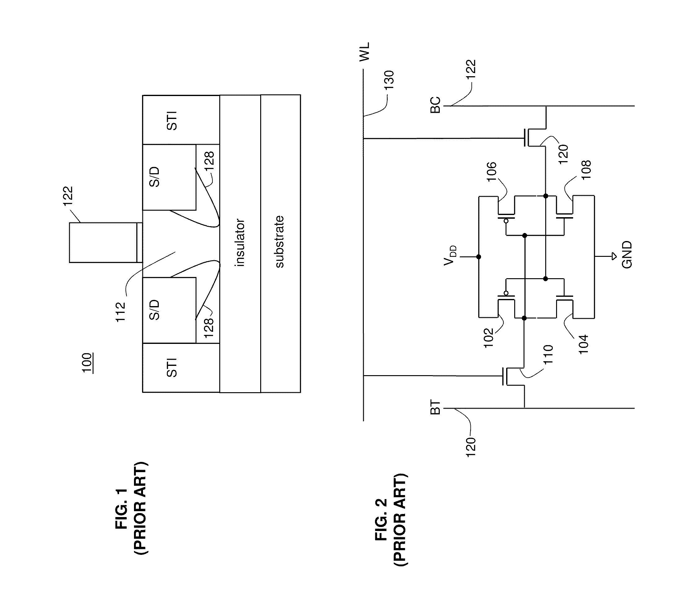
For a given dopant concentration, as the channel length is scaled to smaller dimensions, the FET becomes more susceptible to short channel effects such as punch through.
With symmetrical halo implantation, the device's performance is compromised by the increased junction capacitance and peak electric field caused by the drain side's halo implant.
In an SOI CMOS device, an adjacent p-FET and n-FET are subject to current leakage between the complementary pair of transistors and to the unwanted phenomenon of latch-up.

Method used


Image

  • High density butted junction CMOS inverter,  and making and layout of same
  • High density butted junction CMOS inverter,  and making and layout of same
  • High density butted junction CMOS inverter,  and making and layout of same

Examples


Embodiment Construction

[0045]The exemplary embodiments of the invention and the various features and advantageous details thereof are explained more fully with reference to the non-limiting exemplary embodiments that are illustrated in the accompanying drawings and detailed in the following description. It should be noted that the features illustrated in the drawings are not necessarily drawn to scale. Descriptions of well-known materials, components, and processing techniques are omitted so as to not unnecessarily obscure the exemplary embodiments of the invention. The examples used herein are intended to merely facilitate an understanding of ways in which the exemplary embodiments of the invention may be practiced and to further enable those of skill in the art to practice the exemplary embodiments of the invention. Accordingly, the examples should not be construed as limiting the scope of the exemplary embodiments of the invention.

[0046]As stated above, scaling of silicon-on-insulator (SOI) CMOS ICs to...


PUM


Abstract

A high density, asymmetric, butted junction CMOS inverter, formed on an SOI substrate, may include: an asymmetric p-FET that includes a halo implant on only a source side of the p-FET; an asymmetric n-FET that includes a halo implant on only a source side of the n-FET; and a butted junction comprising an area of said SOI substrate where a drain region of the asymmetric n-FET and a drain region of the asymmetric p-FET are in direct physical contact. Asymmetric halo implants may be formed by a sequential process of covering a first FET of the CMOS inverter with an ion-absorbing structure and applying angled ion radiation to only the source side of the second FET, removing the ion-absorbing structure, covering the first FET with a second ion-absorbing structure, and applying angled ion radiation to only the source side of the second FET. A layout display of CMOS integrated circuit may require one ground rule for the high density, asymmetric butted junction CMOS inverter and another ground rule for other CMOS circuits.

Description

BACKGROUND[0001]1. Field of the Invention[0002]The present invention relates to a high density, butted junction, complementary metal oxide semiconductor (CMOS) inverter, the making of the high density, butted junction CMOS inverter, and ground rules for the layout of the high density, butted junction CMOS inverter in a CMOS integrated circuit including circuits other than the high density, butted junction CMOS inverter. In particular, the high density, butted junction CMOS inverter of the invention comprises two asymmetric field effect transistors (FETs). In particular, the ground rule for the layout of the high density, butted junction CMOS inverter allows for smaller gate-to-gate spacing of the two asymmetric FETs, when compared to the gate-to-gate spacing of FETs used in circuits other than the CMOS inverter of the invention.[0003]2. Description of the Related Art[0004]To decrease size and cost of integrated circuits, semiconductor devices are scaled down and subject to shrinking...

Claims


Application Information

Patent Timeline
Patent Type & Authority Applications(United States)
IPC IPC(8): H01L27/12H01L21/86
CPCH01L21/823807H01L21/823878H01L29/66742H01L27/1203H01L21/84H01L21/26586
Inventor BRYANT, ANDRESCHANG, JOSEPHINE B.SLEIGHT, JEFFREY W.
Owner IBM CORP
Learn More