
Method for manufacturing silicon single crystal, and silicon wafer

a manufacturing method and technology for silicon wafers, applied in the direction of crystal growth process polycrystalline material growth, etc., can solve the problem of not always easy to obtain such single crystals free from defects, and achieve the effect of reducing the generation of characteristic defectives, reducing the generation of defectives, and forming bmd insufficiently and uniformly

Active Publication Date: 2006-10-12
SUMCO CORP
View PDF4 Cites 12 Cited by
  • Summary
  • Abstract
  • Description
  • Claims
  • Application Information

AI Technical Summary

Benefits of technology

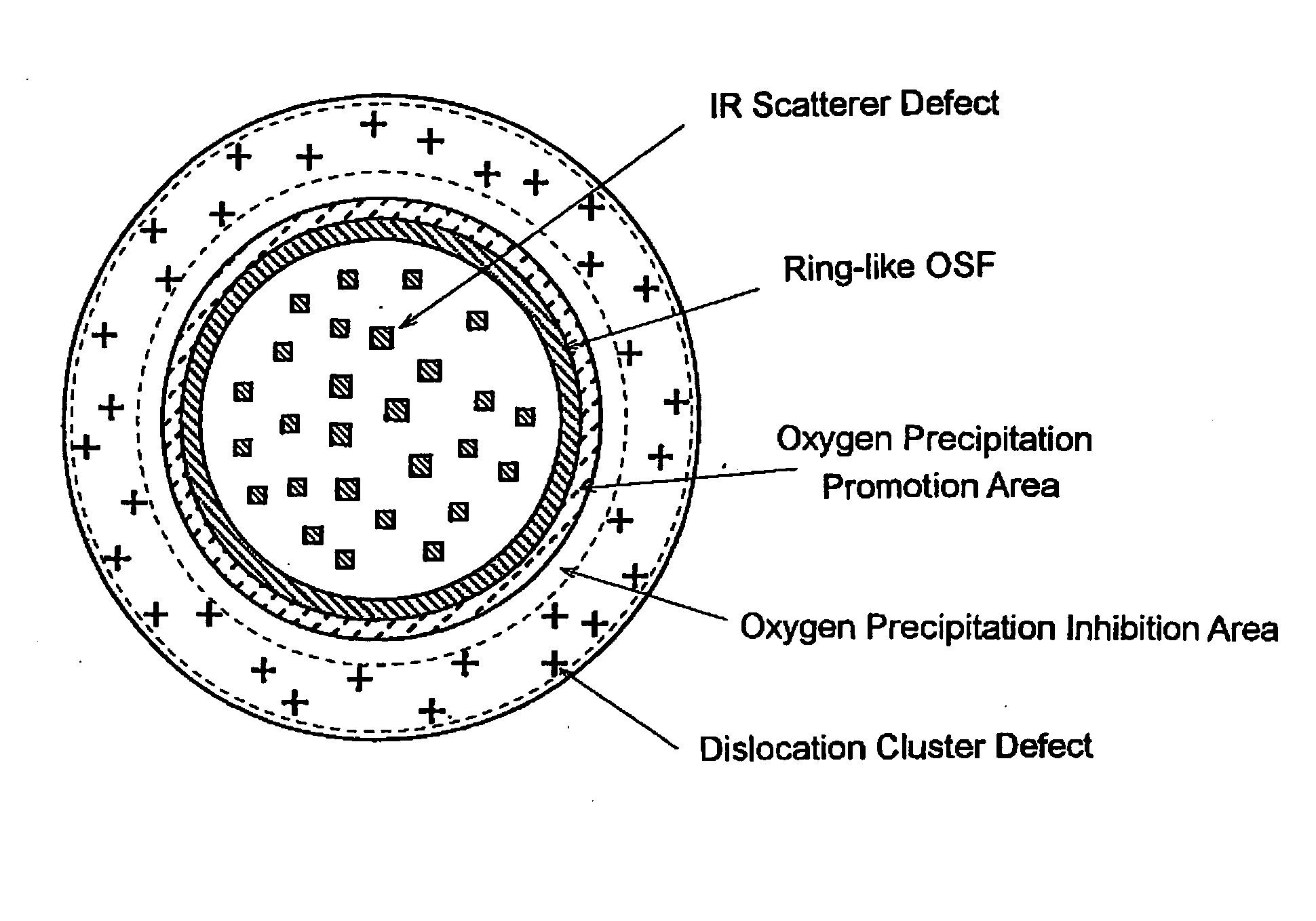
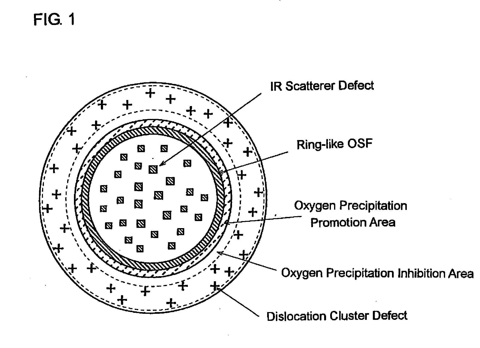
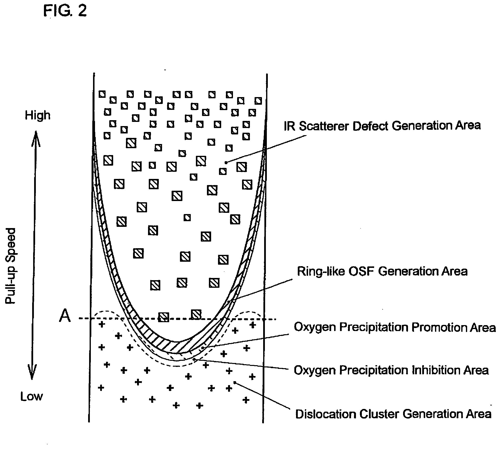
[0026] The present invention relates to a method for manufacturing silicon single crystal composed of a defect-free area free from the Grown-in defects, and a wafer made of the crystal by applying the same. As a technique of growing the defect-free single crystal, it is known to use an apparatus with a hot zone structure adopted so that the temperature gradient in the pulling axial direction of the single crystal just after solidification is larger in the center part than in the outer circumferential part, and limit the pull-up speed to a specific range.
[0028] It is an objective of the present invention to provide a method for manufacturing silicon single crystal which is to easily obtain a wafer with a defect-free area and to generate BMD uniformly and sufficiently and to provide a silicon wafer produced from the single crystal.
[0039] According to the method for manufacturing a silicon single crystal of the present invention, a silicon single crystal for cutting out a wafer, the whole surface of which is composed of the defect-free area free from the Grown-in defects, and which can sufficiently and uniformly form BMD, can be easily manufactured. Such a wafer can significantly reduce generation of characteristic defectives of integrated circuits to be formed thereon and contribute for improving the production yield as a substrate responding to the demand for further miniaturaization and higher density of the circuits.

Problems solved by technology

However, it is not always easy to obtain such single crystals free from defects with sufficient generation of BMD having an intrinsic gettering effect, the BMD formed uniformly over the whole surface in the wafer surface direction.

Method used


Image

  • Method for manufacturing silicon single crystal, and silicon wafer
  • Method for manufacturing silicon single crystal, and silicon wafer
  • Method for manufacturing silicon single crystal, and silicon wafer

Examples


example 1

[0098] A growing experiment was carried out by use of an apparatus having a sectional structure schematically shown in FIG. 6. In this drawing, a heat shielding body 7 has a structure consisting of an outer shell made of graphite and the interia filled with graphite felt therein, with an outer diameter of a portion to be put into a crucible of 480 mm, a minimum inside diameter S at the bottom end of 270 mm, and a radial width W of 105 mm, the inner surface of which is a reverse truncated conical face started from the lower end with an inclination with respect to the vertical direction of 21°. The crucible 1 has an inside diameter of 550 mm, and the height H of the lower end of the heat shielding body 7 from melt surface is 60 mm.

[0099] In this growing apparatus, the heat shielding body 7 is set to have a large thickness for a lower end part thickness and a large height H of its lower endmost from the melt surface, so that the temperature distribution within the single crystal pulle...

example 2

[0105] Using the same growing apparatus as in Example 1, single crystals were grown by varying the pull-up speed from 0.6 mm / min to 0.3 mm / min to 0.6 mm / min at a pressure of the apparatus internal atmosphere of 4000 Pa, wherein the hydrogen partial pressure of the apparatus internal atmosphere and the carbon quantity to be doped to crystals were varied.

[0106] The resulting single crystals were examined for distribution of each defect area in the same manner as in Example 1. The OSF density was examined by optical microscopic observation after heat treatment was performed at 1100° C in dry oxygen atmosphere for 16 hours followed by 3 em-light etching on above section. The growing conditions and examination results are shown in Table 2.

TABLE 2Pull-up speedHydrogenrange (mm / min)OSF densityCarbonpartialDefect-PV +generatedCrystalConcentrationpressure infreeOSFin OSF areaNo.(atoms / cm3)atmosphere (Pa)areaarea(piece / cm2)Notes1*—*—0.03840.02755.2 × 104 Comparative Example92.3 × 1016 400....

example 3

[0109] By use of the same growing apparatus as in Example 1, four kinds of single crystals in total were grown with parameters comprising an apparatus atmospheric gas pressure of 4000 Pa; a hydrogen partial pressure of 160 Pa; and a pull-up speed of 0.397 mm / min capable of making the center of wafer an OSF generation area, wherein two levels of oxygen concentration of 1.0×10¹⁸ atoms / cm3 and 1.3×10¹⁸ atoms / cm3 are made, and wherein the cases with and without doping of carbon to each level of oxygen concentration are included.

[0110] Wafers were cut from the center part of the resulting single crystals, subjected to heat treatment for OSF generation by heating at 1100° C. for 16 hours in dry oxygen atmosphere, and examined for the OSF density at sections. The examination result is shown in FIG. 7.

[0111] In No. 15 with sufficiently low oxygen, OSF is not substantially generated, but in No. 17 with oxygen exceeding 1.2×10¹⁸ atoms / cm3, a number of OSF is generated in the OSF area. In No...


PUM

PropertyMeasurementUnit
partial pressureaaaaaaaaaa

Abstract

A silicon single crystal is manufactured by growing said crystal composed of a defect-free area free from the Grown-in defects by the CZ process, adding a gas of a hydrogen atom-containing substance to an atmosphere gas within a growing apparatus, and doping nitrogen and / or carbon in the crystal. Therefore, a wafer the whole surface of which is composed of the defect-free area free from the Grown-in defects and which can sufficiently and uniformly form BMD can be easily sliced. Such a wafer can be extensively used, since it can significantly reduce generation of characteristic defectives of integrated circuits to be formed thereon and contribute for improving the production yield as a substrate responding to the demand for further miniaturization and higher density of the circuits.

Description

FIELD OF THE INVENTION [0001] The present invention relates to a method for manufacturing silicon single crystal which is a raw material for a silicon wafer used as a substrate for semiconductor integrated circuit, and a silicon wafer produced from the single crystal. DESCRIPTION OF THE PRIOR ART [0002] To manufacture a single crystal of silicon, from which a silicon wafer used for a substrate for semiconductor integrated circuit (device) is cut out, a growing method by the Czochralski process (hereinafter referred to as CZ process) has been most commonly adopted. The CZ process comprises the steps of growing a single crystal by immersing and pulling up seed crystal in and from molten silicon within a quartz crucible, and the progress of this growing technique enables production of a dislocation-free large single crystal with least defects. [0003] A semiconductor device is made into a product through a number of processes for circuit formation by using a wafer obtained from single c...

Claims


Application Information

Patent Timeline
Patent Type & Authority Applications(United States)
IPC IPC(8): C30B15/00C30B21/06C30B27/02C30B28/10C30B30/04
CPCC30B15/04C30B29/06C30B15/203
Inventor ONO, TOSHIAKISUGIMURA, WATARUHOURAI, MASATAKA
Owner SUMCO CORP
Learn More