
C-shaped confinement ring for a plasma processing chamber

a plasma processing chamber and confinement ring technology, applied in vacuum evaporation coatings, electrolysis components, coatings, etc., can solve problems such as plasma extinguishing

Active Publication Date: 2012-01-05
LAM RES CORP
View PDF6 Cites 15 Cited by
  • Summary
  • Abstract
  • Description
  • Claims
  • Application Information

AI Technical Summary

Benefits of technology

[0017]Described herein is a confinement ring useful as a component of a capacitively-coupled plasma processing chamber wherein inner surfaces of the confinement ring provide an extended plasma confinement zone surrounding a gap between an upper electrode and a lower electrode on which a semiconductor substrate is supported during plasma processing in the chamber, the confinement ring comprising: an upper annular wall which extends horizontally and includes an annular flange at an inner end thereof adapted to underlie an outer edge of the upper electrode of the plasma chamber; a sidewall extending vertically downward from an outer end of the upper wall; and a lower annular wall extending horizontally inward from a lower end of the sidewall, the lower wall including circumferentially spaced apart radially extending slots, each of the slots having a length of at least 1.0 inch and a uniform width of 0.05 to 0.2 inch, the slots being evenly spaced at radial positions offset by no more than 2°.

Problems solved by technology

Too high a chamber pressure can disadvantageously contribute to etch stop while too low a chamber pressure can lead to plasma extinguishment.

Method used


Image

  • C-shaped confinement ring for a plasma processing chamber
  • C-shaped confinement ring for a plasma processing chamber
  • C-shaped confinement ring for a plasma processing chamber

Examples


Embodiment Construction

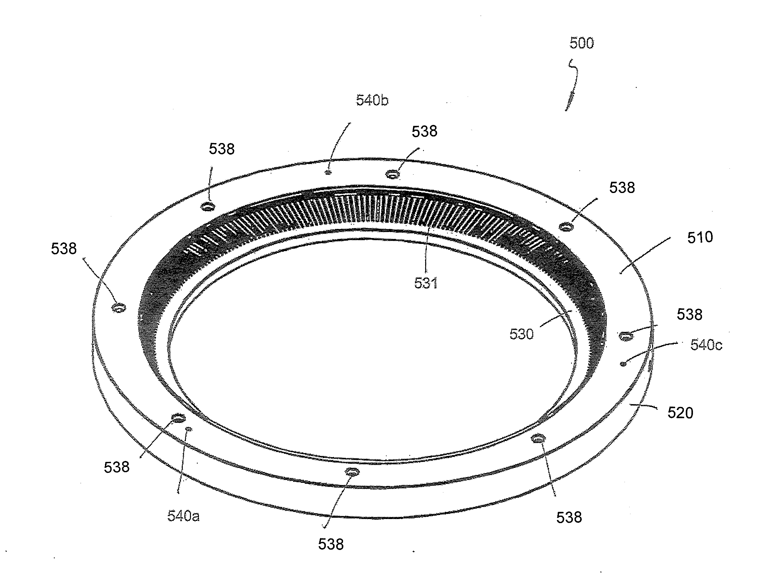
[0027]Described herein is a confinement ring configured to confine plasma in an extended plasma confinement zone surrounding a gap between an upper electrode and a lower electrode of an adjustable gap capacitively-coupled plasma processing chamber. FIG. 3 shows a partial cross section of an exemplary adjustable gap capacitively-coupled plasma processing chamber 300. The chamber 300 comprises a substrate support assembly 310, an upper electrode including a center electrode plate 303 and an annular outer electrode 304 and an electrically conductive (e.g. pure aluminum or aluminum alloy collectively referred to herein as aluminum) confinement ring 500, according to an embodiment, extending outwardly from the annular outer electrode 304. The confinement ring 500 is C-shaped in cross section when viewed in a vertical plane passing through a center axis thereof.

[0028]FIGS. 4A-4F show details of the confinement ring 500. The confinement ring 500 comprises an upper annular wall 510 which ex...


PUM

PropertyMeasurementUnit
widthaaaaaaaaaa
lengthaaaaaaaaaa
diametersaaaaaaaaaa

Abstract

Described herein is a confinement ring useful as a component of a capacitively-coupled plasma processing chamber. Inner surfaces of the confinement ring provide an extended plasma confinement zone surrounding a gap between an upper electrode and a lower electrode on which a semiconductor substrate is supported during plasma processing in the chamber.

Description

BACKGROUND[0001]With each successive semiconductor technology generation, wafer diameters tend to increase and transistor sizes decrease, resulting in the need for an ever higher degree of accuracy and repeatability in substrate processing. Semiconductor substrate materials, such as silicon wafers, are routinely processed using plasma processing chambers. Plasma processing techniques include sputter deposition, plasma-enhanced chemical vapor deposition (PECVD), resist strip, and plasma etch. Plasma can be generated by subjecting suitable process gases in a plasma processing chamber to radio frequency (RF) power. Flow of RF current in the plasma processing chamber can affect the processing.[0002]A plasma processing chamber can rely on a variety of mechanisms to generate plasma, such as inductive coupling (transformer coupling), helicon, electron cyclotron resonance, capacitive coupling (parallel plate). For instance, high density plasma can be produced in a transformer coupled plasma...

Claims


Application Information

Patent Timeline
Patent Type & Authority Applications(United States)
IPC IPC(8): C23F1/08C23C14/34C23C16/50
CPCH01J37/32091H01J37/32642H01J37/32623
Inventor KELLOGG, MICHAEL C.MARAKHTANOV, ALEXEIDHINDSA, RAJINDER
Owner LAM RES CORP
Features
  • Generate Ideas
  • Intellectual Property
  • Life Sciences
  • Materials
  • Tech Scout
  • Unparalleled Data Quality
  • Higher Quality Content
  • 60% Fewer Hallucinations
Learn More