Light-emitting semiconductor device, mounted substrate, and fabrication method thereof

a technology of semiconductor devices and substrates, applied in semiconductor devices, semiconductor/solid-state device details, electrical devices, etc., can solve the problems of reducing the service life of chips, weak against light and heat, discoloration and degradation of epoxy resins, etc., to prevent the reduction of reflector reflectance and corrosion, improve gas transmission resistance, and prolong the effect of service li

Active Publication Date: 2012-01-12
SHIN ETSU CHEM IND CO LTD
View PDF23 Cites 34 Cited by
  • Summary
  • Abstract
  • Description
  • Claims
  • Application Information

AI Technical Summary

Benefits of technology

[0076]According to the present invention, it is possible to prevent a reduction in the reflectance of a reflector and corrosion, which may occur as a result of penetration of corrosive gas, by significantly improving the gas transmission resistance, and hence to provide a light-emitting semiconductor device capable of assuring long-term reliability.

Problems solved by technology

Keeping in step with the adoption of LEDs with higher brightness and higher power in recent years, the problem of discoloration and degradation of epoxy resins has arisen.
In particular, transparent epoxy resins undergo yellowing by blue light and ultraviolet rays, and therefore, are accompanied by the problem that they reduce the service life of chips.
An organic resin, however, involves a problem in that it is weak against light and heat and is inferior in long-term reliability.
However, the glass with Si—N bonds contained therein has not been allowed to react completely, and therefore is unstable.
As a result of changes with time through hydrolysis or the like, the glass film is lowered in flexibility to form microcracks, leading to problems that damages to the package may be caused or the gas barrier properties of the glass film may be lowered.
These silicone resins are, however, accompanied by problems that in cured forms, they have higher gas transmission property and lower strength than epoxy resins.
However, these high-hardness rubbery silicone resins are low in adhesive properties, and therefore, involve a problem in that, in encased light-emitting semiconductor devices, i.e., devices with light-emitting chips being arranged in ceramic and / or plastic casings and with the casings being internally filled up with the silicone resins, the silicone resins separate from the ceramics or plastics of the casings in thermal shock tests at from −40 to 120° C.
However, this silicone resin is synthesized by subjecting an epoxy-containing silane and a silanol to condensation, and its cured product is low in modulus of elasticity and is brittle.
Therefore, an LED molded in a resin of this type is accompanied by a problem that the resin is prone to cracking in a temperature cycling test.
Neither of these composition are, however, considered to exhibit any satisfactory anti-cracking properties in temperature cycling tests of their cured products.

Method used


Image

  • Light-emitting semiconductor device, mounted substrate, and fabrication method thereof
  • Light-emitting semiconductor device, mounted substrate, and fabrication method thereof
  • Light-emitting semiconductor device, mounted substrate, and fabrication method thereof

Examples


example 1

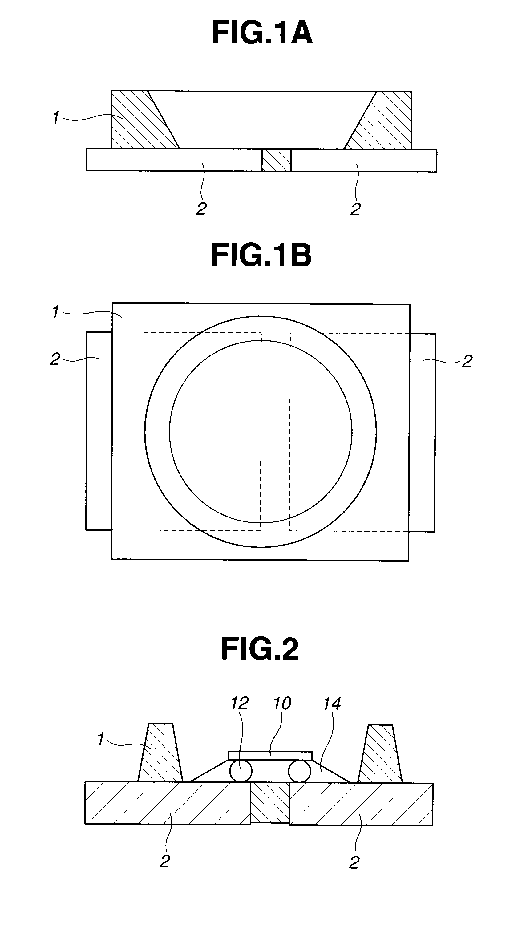
[0121]On a reflector molded with a thermosetting silicone resin composition (“SWC7200T,” trade name, product of Shin-Etsu Chemical Co., Ltd.) and having the structure of FIGS. 1A and 1B, a blue LED was held in place with a silicone-based die bonding material (“KJR-632DA-1,” trade name, product of Shin-Etsu Chemical Co., Ltd.). By heating at 150° C. for one hour, the blue LED was fixed on a die pad.

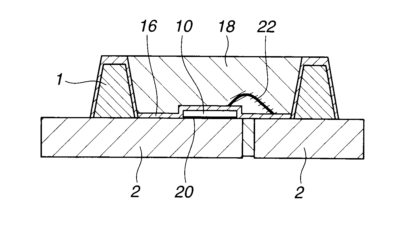
[0122]Subsequently, the blue LED and lead electrodes were electrically connected together via gold wires (FIG. 6). A silicone resin composition, which had been prepared by adding a YAG phosphor at 5 wt % to a transparent silicone resin composition (“LPS-3410,” trade name, product of Shin-Etsu Chemical Co., Ltd.), was then poured into-a recessed part of the reflector by potting. The silicone resin composition was heated and cured at 120° C. for one hour and further at 150° C. for two hours to encapsulate the blue LED.

[0123]The resulting light-emitting semiconductor device was spray-coated w...

example 2

[0125]On a reflector molded from the thermosetting silicone resin composition (“SWC7200T,” trade name, product of Shin-Etsu Chemical Co., Ltd.) and having the structure of FIGS. 1A and 1B, a blue LED was connected via gold bumps as shown in FIG. 2. After the connection, the transparent silicone resin composition (“LPS-3410,” trade name, product of Shin-Etsu Chemical Co., Ltd.), which contained 50 wt % of spherical silica of 5 μm in average particle size, was poured into a gap between the blue LED and a lead frame, and was then cured at 120° C. for one hour. After the silicone resin composition had cured, a 25 wt % solution of perhydropolysilazane (“AQUAMICA”) in tetrabutyl ether was poured into a recessed part of the reflector, followed by curing at 180° C. for 30 minutes. Subsequently, the perhydropolysilazane solution was poured again, and perhydropolysilazane was cured at 180° C. for one hour such that a crack-free, transparent, cured silicon oxide film was formed with an average...

example 3

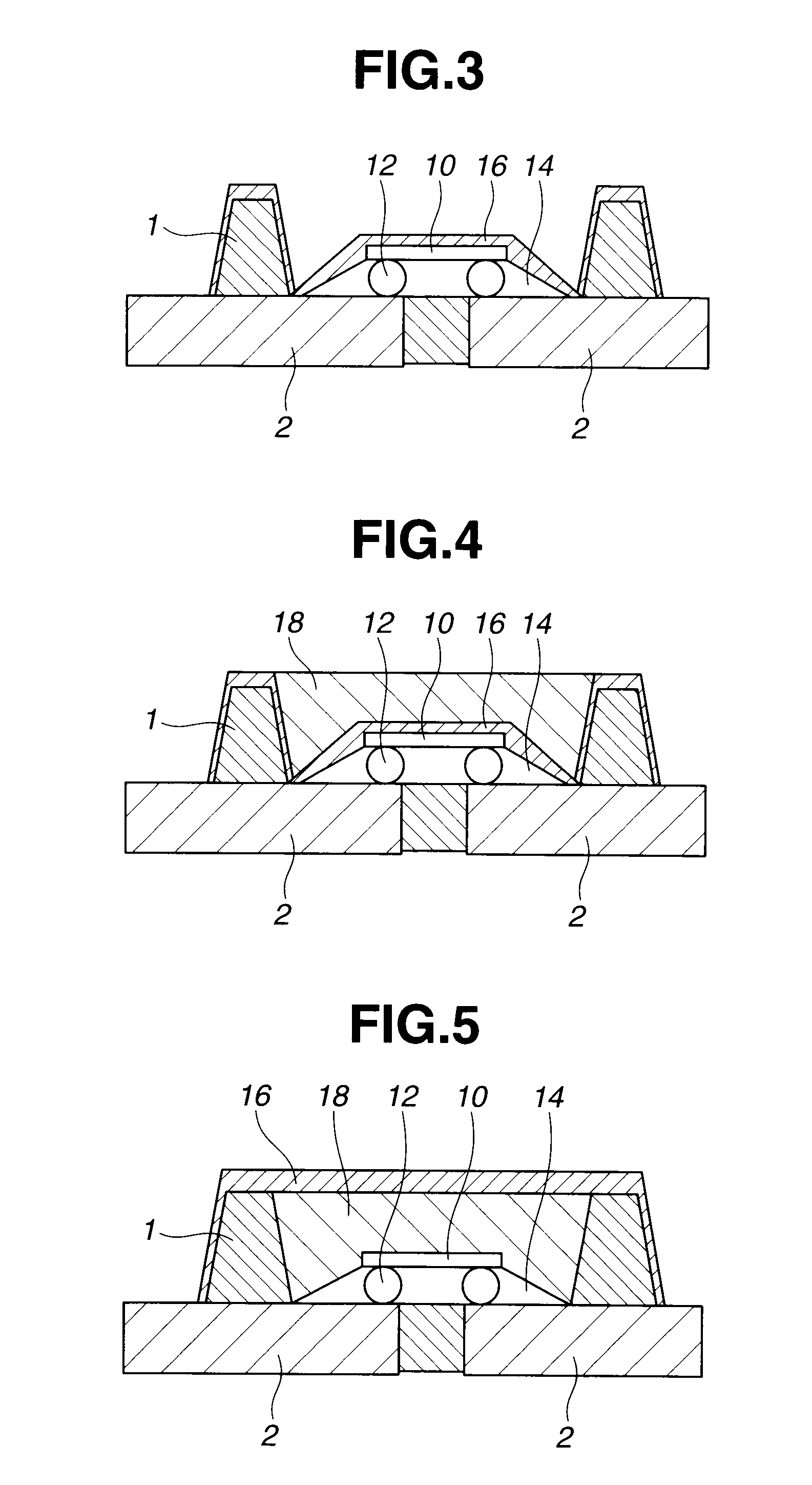
[0126]Using a light-emitting semiconductor device fabricated in a similar manner as Light-emitting semiconductor device No. 3, the same addition curable silicone resin composition as in Example 1 was poured into a recessed part of a reflector by potting, and was then heated and cured at 120° C. for one hour and further at 150° C. for two hours to encapsulate the light-emitting semiconductor device (FIG. 4). The resulting light-emitting semiconductor device was provided as Light-emitting semiconductor device No. 4.


PUM


Abstract

A light-emitting semiconductor device includes a lead frame having lead electrodes, a reflector arranged with the lead frame, and a light-emitting semiconductor chip accommodated in the reflector and having electrodes connected to the lead electrodes by a flip-chip bonding method, wherein: a gap between the lead frame and the light-emitting semiconductor chip is filled with a cured underfill material, and a cured silicon oxide film of 0.05 to 10 μm thickness is formed covering surfaces of the light-emitting semiconductor chip and reflector.

Description

CROSS-REFERENCE TO RELATED APPLICATION[0001]This non-provisional application claims priority under 35 U.S.C. §119(a) on Patent Application No. 2010-155362 filed in Japan on Jul. 8, 2010, the entire contents of which are hereby incorporated by reference.TECHNICAL FIELD[0002]This invention relates to a light-emitting semiconductor device which, owing to significant improvements in gas transmission resistance, can avoid a reduction in brightness associated with a decrease in the reflectance of a reflector and also corrosion due to penetration of corrosive gas, and therefore, can assure long-term reliability. This invention also relates to a fabrication method of the light-emitting semiconductor device, a mounted substrate with the light-emitting semiconductor device mounted thereon, and a fabrication method of the mounted substrate.BACKGROUND ART[0003]Epoxy resin compositions and silicone resin compositions have heretofore been widely used to encapsulate light-emitting semiconductor ch...

Claims


Application Information

Patent Timeline
Patent Type & Authority Applications(United States)
IPC IPC(8): H01L33/60
CPCH01L33/44H01L33/60H01L2933/0025H01L2224/48091H01L2224/45144H01L2224/8592H01L2224/73265H01L2224/73204H01L2924/00014H01L2924/00
Inventor SHIOBARA, TOSHIOKASHIWAGI, TSUTOMU
Owner SHIN ETSU CHEM IND CO LTD
Why Eureka
Try Eureka