Improved on/off ratio for non-volatile memory device and method

a non-volatile memory and on/off ratio technology, applied in the direction of bulk negative resistance effect devices, basic electric elements, electrical equipment, etc., can solve the problem of prohibitively high cost of fabricating such masks, and achieve the effect of a broader range of applicability and fast switching

Active Publication Date: 2012-01-19
CROSSBAR INC
View PDF1 Cites 101 Cited by
  • Summary
  • Abstract
  • Description
  • Claims
  • Application Information

AI Technical Summary

Benefits of technology

[0005]The present invention is in general related to switching devices. More particularly, embodiments of the present provide a method and a structure for a resistive switching device. The resistive switching device

Problems solved by technology

But the cost of fabricating such

Method used


Image

  • Improved on/off ratio for non-volatile memory device and method
  • Improved on/off ratio for non-volatile memory device and method
  • Improved on/off ratio for non-volatile memory device and method

Examples


Embodiment Construction

[0012]The present invention is in general related to switching devices. More particularly, embodiments of the present invention provide a method and a structure for a resistive switching device. The resistive switching device may be used in non-volatile memory devices that provide for random access, fast switching, and are scalable to very small sizes. But it should be recognized that the present invention can have a much broader range of applicability.

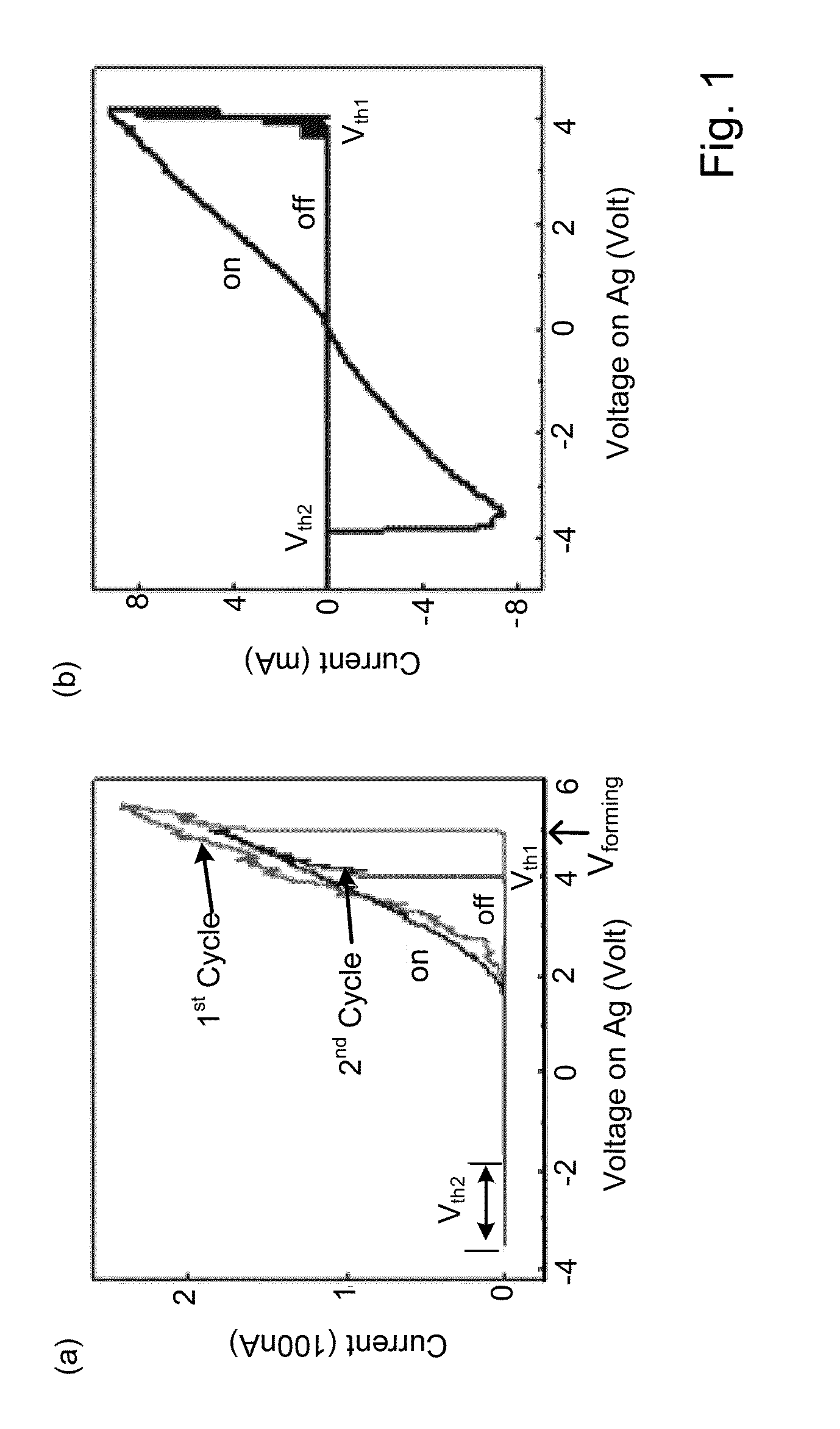
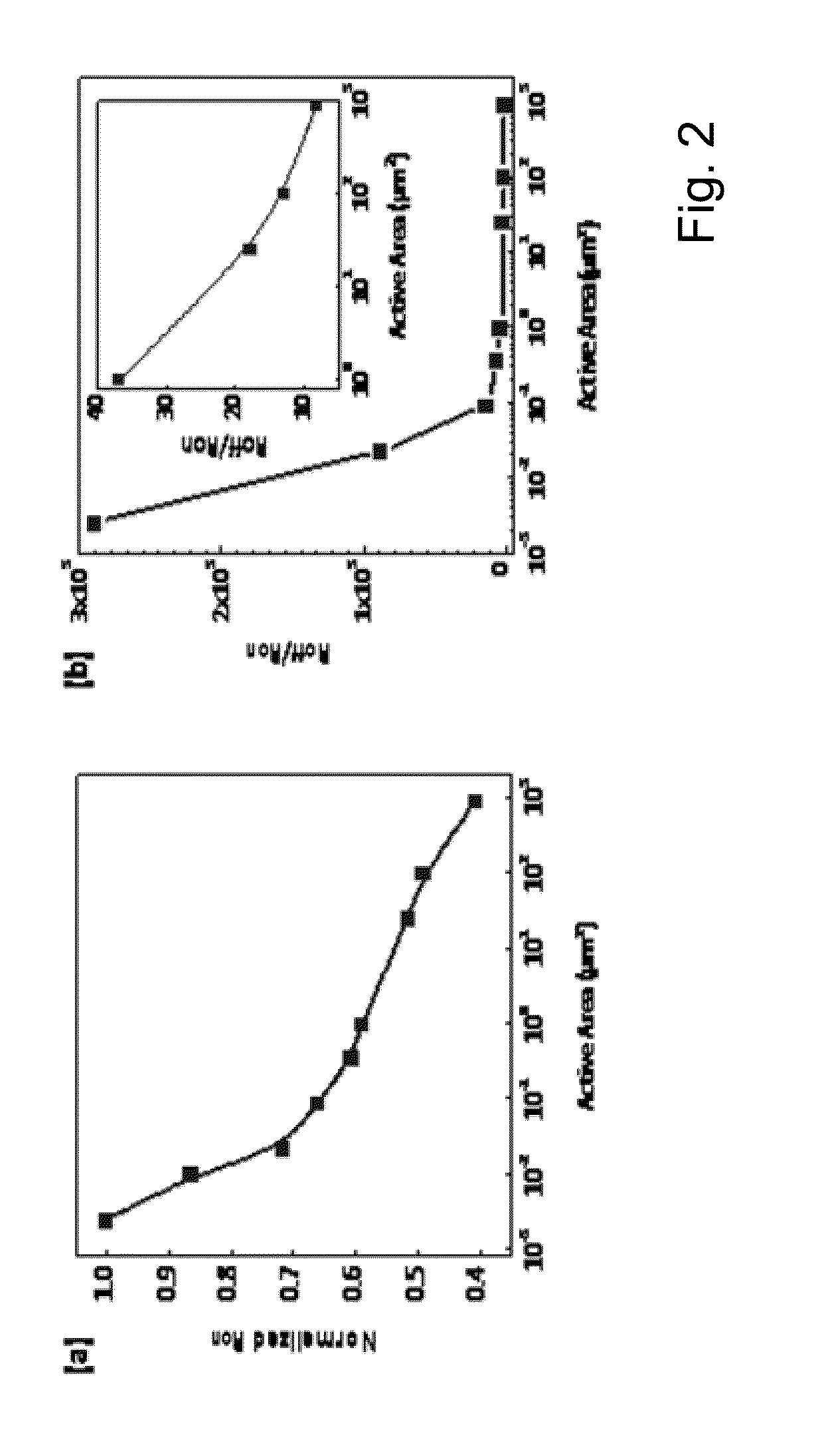
[0013]Resistive switching behavior has been observed and studied in micrometer-scale amorphous silicon (a-Si) devices since the 1980s. A typical device consists of a pair of metal electrodes sandwiching an amorphous-Si layer in a so-called Metal / a-Si / Metal (M / a-Si / M) structure, in which the voltage applied across the pair of metal electrodes may cause changes in the a-Si resistance. These conventional M / a-Si / M based nonvolatile switching devices have the advantages of high Ion / Ioff ratios, and can be fabricated with a CMOS compatible ...


PUM


Abstract

This application describes a method of forming a switching device. The method includes forming a first dielectric material overlying a surface region of a substrate. A bottom wiring material is formed overlying the first dielectric material and a switching material is deposited overlying the bottom wiring material. The bottom wiring material and the switching material is subjected to a first patterning and etching process to form a first structure having a top surface region and a side region. The first structure includes at least a bottom wiring structure and a switching element having a top surface region including an exposed region of the switching element. A second dielectric material is formed overlying at least the first structure including the exposed region of the switching element. The method forms a first opening region in a portion of the second dielectric layer to expose a portion of the top surface region of the switching element. A dielectric side wall structure is formed overlying a side region of the first opening region. A top wiring material including a conductive material is formed overlying at lease the top surface region of the switching element such that the conductive material is in direct contact with the switching element. The side wall spacer reduces a contact area for the switching element and the conductive material and thus a reduced active device area for the switching device. In a specific embodiment, the reduced area provides for an increase in device ON/OFF current ratio.

Description

BACKGROUND[0001]The present invention is in general related to switching devices. More particularly, embodiments of the present invention provide a method and a structure for a resistive switching device. The resistive switching device can be used in a non-volatile resistive switching memory device with random access and fast switching characteristics.[0002]Semiconductor memory cells usually include a transistor device. Scaling of memory devices is therefore driven by reducing the size of the transistor. However, fundamental difficulties with scaling commonly used memory cells, such as those using floating gates, are driving the industry to examine a new memory cell structure that will allow scaling to ever smaller dimensions. New classes of memory devices being actively investigated include ferroelectric RAM (Fe RAM), magneto-resistive RAM (MRAM), organic RAM (ORAM), and phase change RAM (PCRAM). These devices usually attempt to use new materials and combine with silicon based devi...

Claims


Application Information

Patent Timeline
IPC IPC(8): H01L45/00H01L21/02
CPCH01L45/148H01L45/085H01L45/1233H01L45/1273H01L45/16H01L45/1675H01L45/06H01L45/1266H10N70/245H10N70/8416H10N70/884H10N70/011H10N70/063H10N70/826H10N70/8418H10N70/231
Inventor HERNER, SCOTT BRAD
Owner CROSSBAR INC
Why Eureka
Try Eureka