Semiconductor device

Inactive Publication Date: 2012-01-19
SEMICON ENERGY LAB CO LTD
View PDF1 Cites 15 Cited by
  • Summary
  • Abstract
  • Description
  • Claims
  • Application Information

AI Technical Summary

Benefits of technology

[0025]Since the off-state current of a transistor including an oxide semiconductor is extremely low, stored data can be held for an extremely long time by using the transistor. In other words, power consumption can be significantly reduced because refresh operation becomes unnecessary or the frequency of refresh operation can be extremely low. Moreover, stored data can be held for a long period even when no power is supplied (note that an electric potential is preferably fixed).
[0026]Further, a semiconductor device according to one embodiment of the disclosed invention does not need high voltage for writing of data and there is no problem of deterioration of elements. For example, unlike a conventional non-volatile memory, it is not necessary to inject and extract electrons into and from a floating gate, and thus a problem such as deterioration of a gate insulating layer does not occur at all. In other words, the semiconductor device according to one embodiment of the

Problems solved by technology

Moreover, since leakage current (off-state current) or the like flows between a source and a drain of a transistor included in a memory element when the transistor is in an off state, charge flows into or out even if the transistor is not selected, which makes a data holding period short.
For this reason, another writing operation (refresh operation) is necessary at predetermined intervals, and it is difficult to sufficiently reduce power consumption.
Furthermore, since stored data is lost when no power is supplied, an additional memory device using a magnetic material or an optical material is needed in order to hold the data for a long time.
However, cost per storage capacity is increased because a circuit such as a flip-flop is used.
Mor

Method used


Image

  • Semiconductor device
  • Semiconductor device
  • Semiconductor device

Examples


embodiment 1

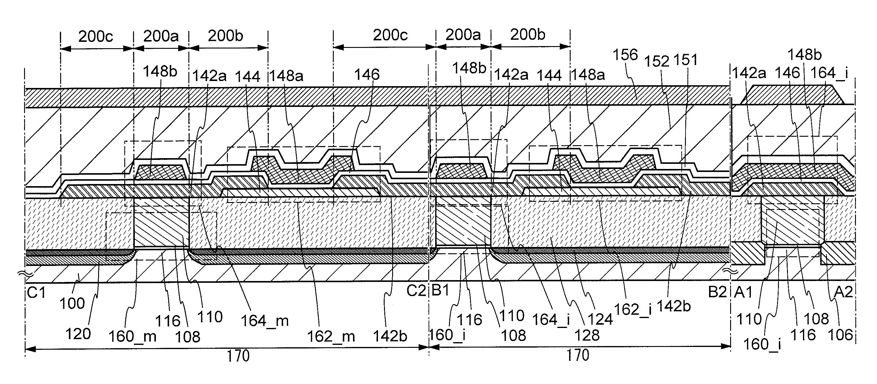
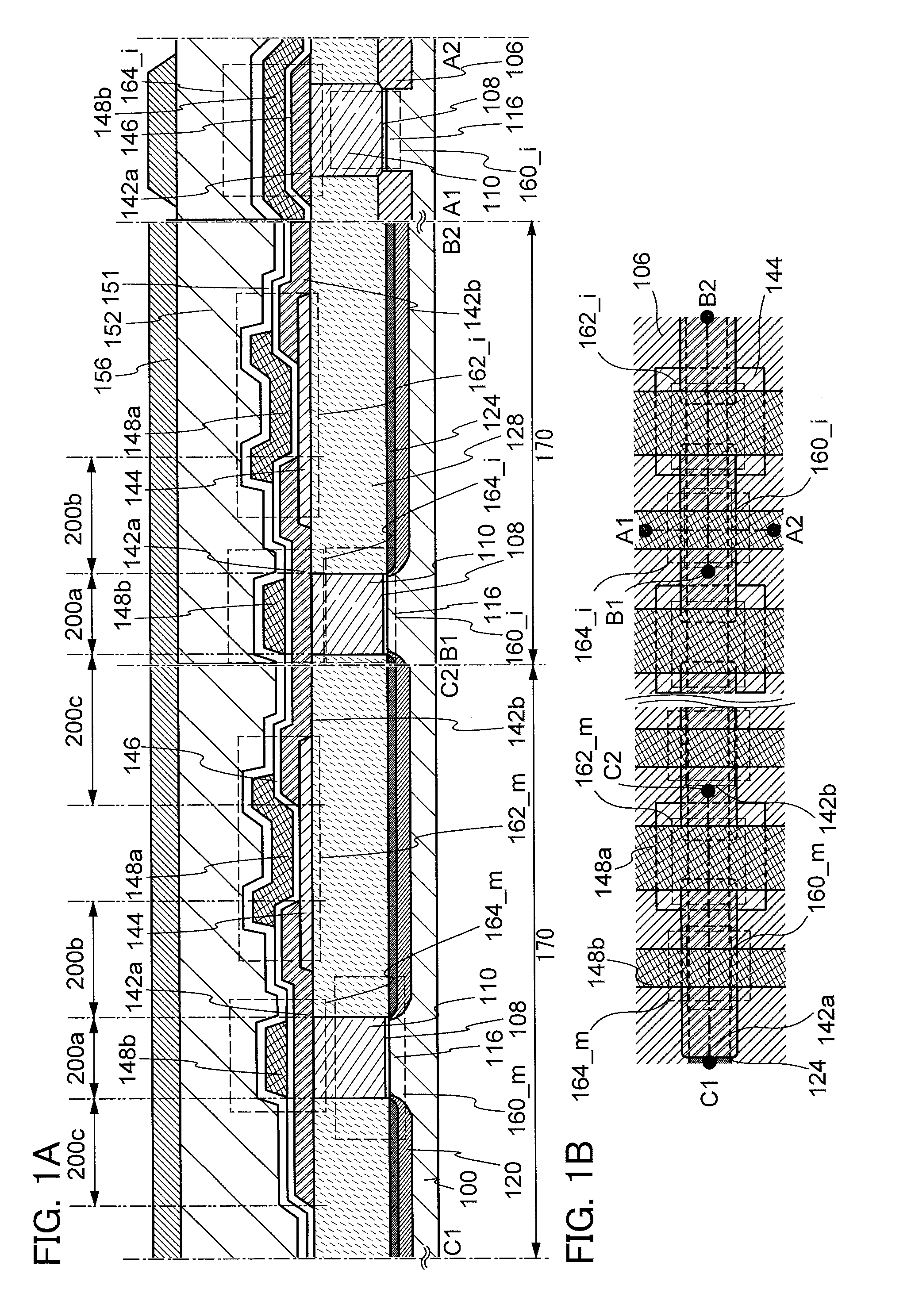
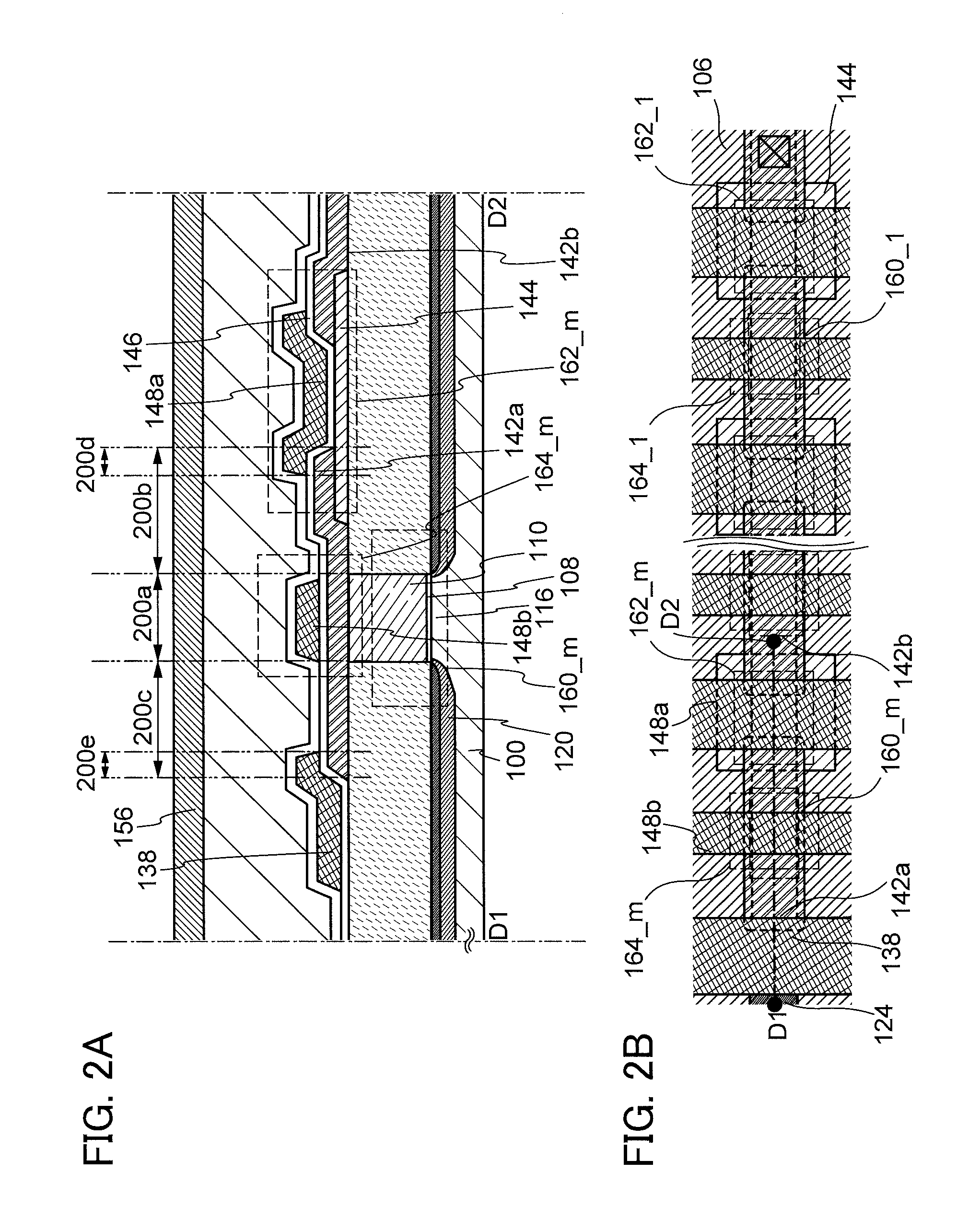
[0043]In this embodiment, a circuit configuration and an operation according to one embodiment of the disclosed invention will be described with reference to drawings. Note that in some circuit diagrams, “OS” is written beside a transistor in order to indicate that the transistor includes an oxide semiconductor. In addition, a structure and a manufacturing method of a semiconductor device to which the circuit configuration is applied are described with reference to drawings.

[0044]First, a basic circuit configuration and an operation thereof will be described with reference to FIGS. 7A to 7C. In a semiconductor device illustrated in FIG. 7A, a first wiring (1st Line) is electrically connected to a source electrode (or a drain electrode) of a transistor 160. A second wiring (2nd Line) is electrically connected to the drain electrode (or the source electrode) of a transistor 160. A third wiring (3rd Line) is electrically connected to a source electrode (or a drain electrode) of a trans...

application example

[0070]Next, a more specific circuit structure to which the circuit illustrated in FIGS. 7A to 7C is applied and an operation thereof will be described with reference to FIG. 8 and FIGS. 9A to 9C.

[0071]A semiconductor device illustrated in FIG. 8 is an example of a circuit diagram of a semiconductor device including m memory cells 170. The structure of the memory cells 170 in FIG. 8 is similar to that in FIG. 7A. That is, the first wiring in FIG. 7A corresponds to a bit line 13L in FIG. 8; the second wiring in FIG. 7A, a source line SL in FIG. 8; the third wiring in FIG. 7A, a signal line S in FIG. 8; the fourth wiring in FIG. 7A, a write word line WWL in FIG. 8; and the fifth wiring in FIG. 7A, a read word line RWL in FIG. 8. FIG. 8 is a circuit diagram of a so-called NAND type semiconductor device in which the memory cells 170 are connected in series between the bit line BL and the source line SL. In the configuration of FIG. 8, the bit line BL and the drain electrode of the transi...

embodiment 2

[0201]In this embodiment, electronic devices to which the semiconductor device described in Embodiment 1 is applied to will be described with reference to FIGS. 10A to 10F. In this embodiment, the above-described semiconductor device is applied to electronic devices such as computers, mobile phone sets (also referred to as mobile phones o mobile phone devices), portable information terminals (including portable game machines, audio reproducing devices, and the like), digital cameras, digital video cameras, electronic paper, television sets (also referred to as televisions or television receivers), and the like.

[0202]FIG. 10A illustrates a notebook personal computer, which includes a housing 701, a housing 702, a display portion 703, a keyboard 704, and the like. The semiconductor device described in Embodiment 1 is provided in at least one of the housings 701 and 702. Thus, a notebook personal computer with sufficiently low power consumption, in which writing and reading of data can...


PUM


Abstract

A semiconductor device with a novel structure is provided, which can hold stored data even when no power is supplied and which has no limitations on the number of writing operations. A semiconductor device is formed using a material which enables off-state current of a transistor to be reduced significantly; e.g., an oxide semiconductor material which is a wide-gap semiconductor. With use of a semiconductor material which enables off-state current of a transistor to be reduced significantly, the semiconductor device can hold data for a long period. In a semiconductor device with a memory cell array, parasitic capacitances generated in the nodes of the first to the m-th memory cells connected in series are substantially equal, whereby the semiconductor device can operate stably.

Description

TECHNICAL FIELD[0001]The disclosed invention relates to a semiconductor device using a semiconductor element and a method for driving the semiconductor device.BACKGROUND ART[0002]Memory devices including semiconductor elements are broadly classified into two categories: volatile memory devices that cannot hold stored data when not powered, and nonvolatile memory devices that hold stored data even when not powered.[0003]A typical example of volatile memory devices includes a DRAM (dynamic random access memory). A DRAM stores data in such a manner that a transistor included in a memory element is selected to store electric charge in a capacitor.[0004]On the above-described principle, when data is read from a DRAM, charge in a capacitor is lost; thus, another writing operation is necessary every time data is read out. Moreover, since leakage current (off-state current) or the like flows between a source and a drain of a transistor included in a memory element when the transistor is in ...

Claims


Application Information

Patent Timeline
IPC IPC(8): H01L27/108
CPCG11C16/0433G11C16/26H01L29/78H01L27/1156H01L27/11517H10B41/00H10B41/70
Inventor KATO, KIYOSHIMATSUZAKI, TAKANORINAGATSUKA, SHUHEIINOUE, HIROKI
Owner SEMICON ENERGY LAB CO LTD
Why Eureka
Try Eureka