

Organic semiconductors capable of ambipolar transport
- Summary
- Abstract
- Description
- Claims
- Application Information
AI Technical Summary
Benefits of technology
Problems solved by technology
Method used
Image

Examples
examples
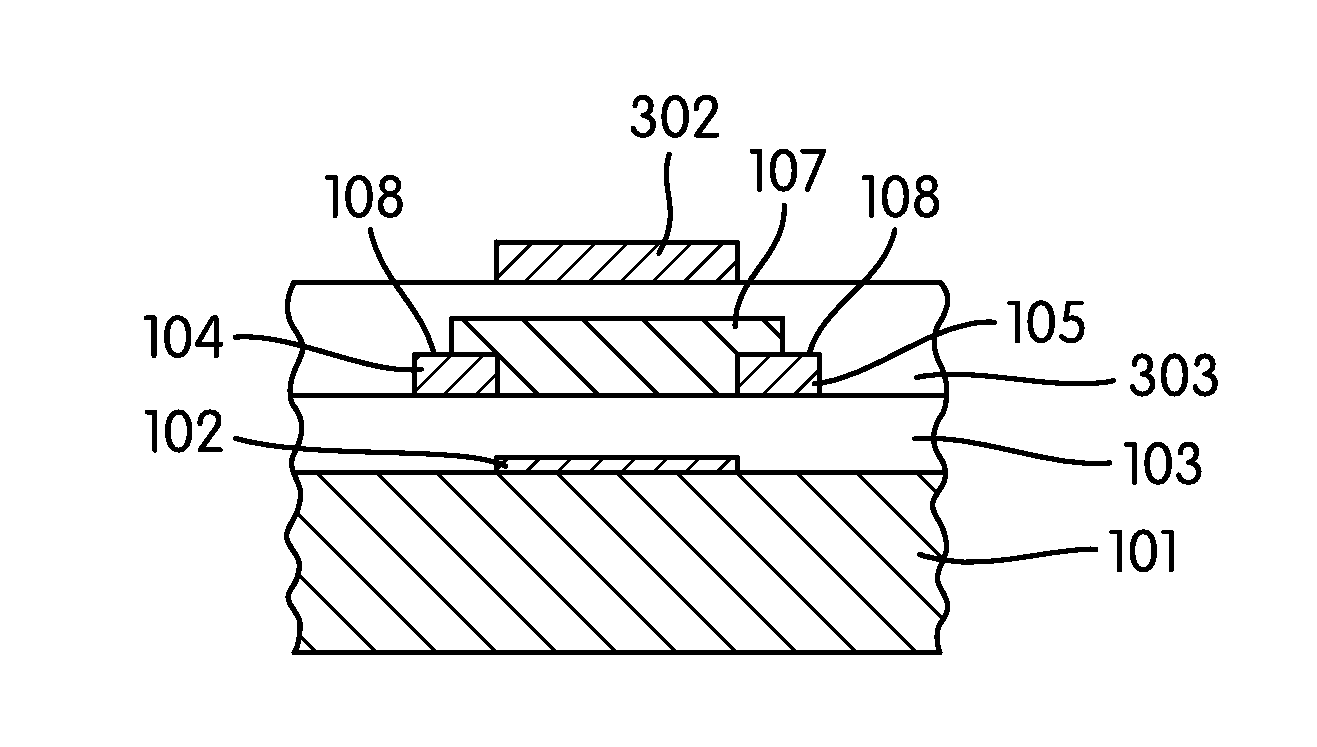
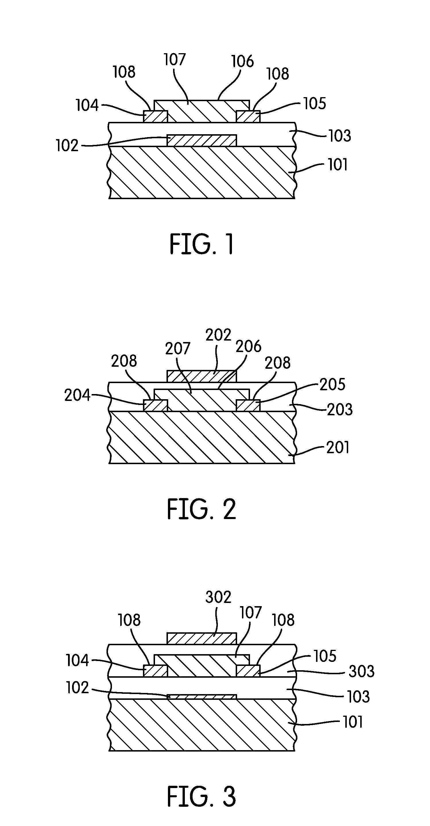
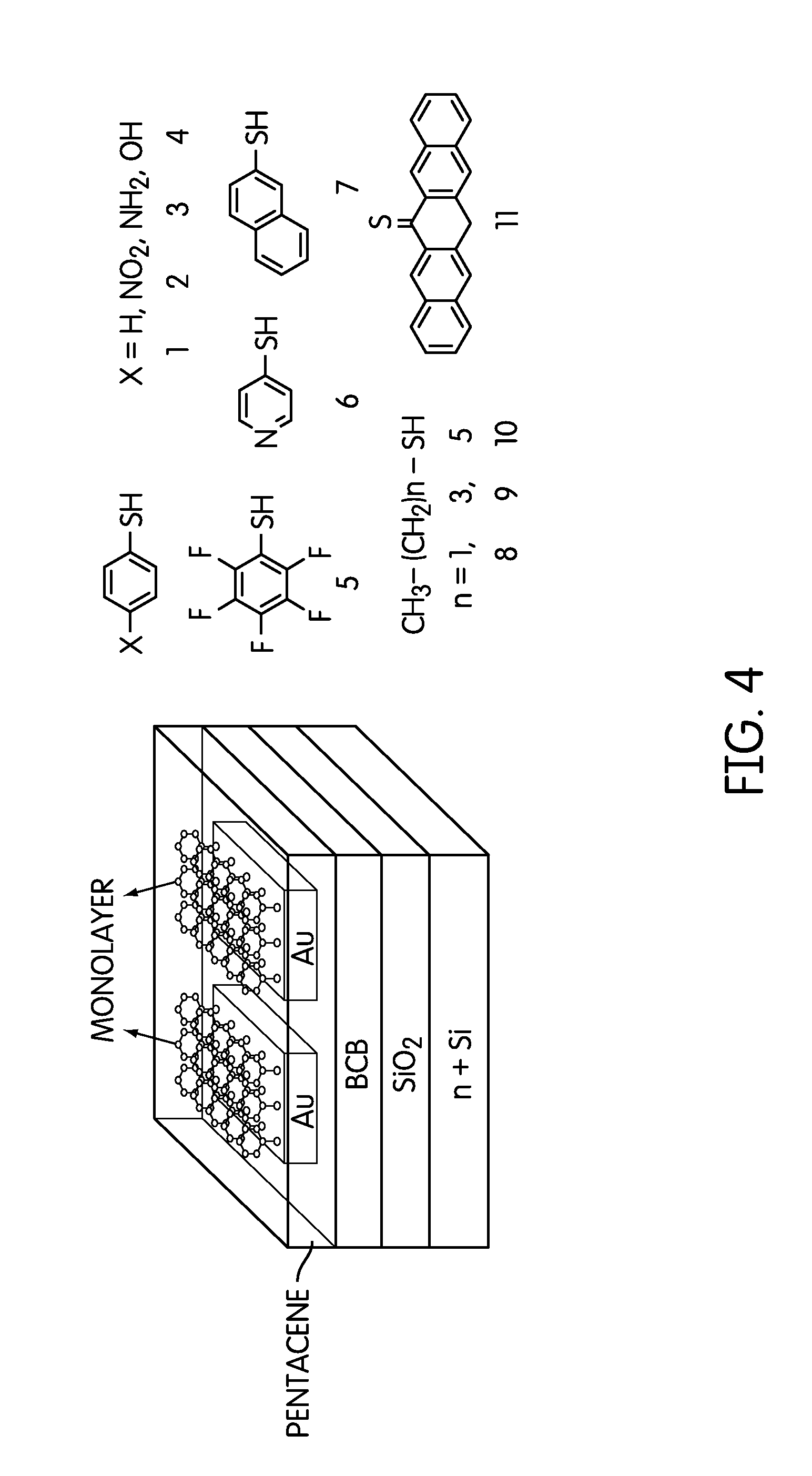
[0038]Pentacene FETs were fabricated in bottom contact geometry, as illustrated in FIG. 4. N-type Si wafers (ρ2 served as the back gate and part of the gate-dielectric stack of the FETs, respectively. The substrates were transferred into a N2-glove box where all the device fabrication and characterization was performed. The wafers were cleaned by UV-ozone for 20 min. A 1:3 solution of BCB:mesitylene was filtered (0.2 μm polytetrafluoroethylene (PTFE) syringe filter), deposited by spin-coating at 3000 rpm for 30 s, and annealed at 265° C. for 30 s, providing a BCB (benzocyclobutene) layer about 130 nm thick. The measured capacitance of the SiO2 (250 nm) / BCB (˜130 nm) gate dielectric stack was 7.6(±0.25) nF / cm2. Au source and drain electrodes (15-20 nm in thickness) were thermally evaporated through a shadow mask to define channel lengths (L) ranging from 30-200 μm and widths (W) to provide W / L of 15 for each device.
[0039]Benzenethiol (1), 4-nitrobenzenethiol (2), 4-aminobenzenethiol ...
PUM
 Abstract
Description
Claims
Application Information