Process for electrodeposition of copper chip to chip, chip to wafer and wafer to wafer interconnects in through-silicon vias (TSV) with heated substrate and cooled electrolyte

Inactive Publication Date: 2012-02-02
ATOTECH DEUT GMBH
View PDF4 Cites 13 Cited by
  • Summary
  • Abstract
  • Description
  • Claims
  • Application Information

AI Technical Summary

Benefits of technology

[0035]As described in summary in the foregoing, and in detail in the following, in various of its embodiments, the present invention avoids the disadvantages of known processes and, more particularly, maximizes the rate of electrodepositing the metal fill of the TSVs with a metal such as highly pure copper while at the same time the invention minimizes stress, avoids defects such as inclusions and voids, and other defects, which have been found in prior art TSVs. The present invention therefore addresses and provides a solution to the problem of improving the rate of electrodeposition of metals for TSV

Problems solved by technology

TSVs have been used for forming electrical connections between respective layers in a stacked or 3D arrangement in devices such as MEMS and semiconductor devices, but have suffered from various defects arising, at least partially, from difficulty in electroplating highly pure copper into the very large, high aspect ratio vias in the TSVs.
Attempts to electrodeposit high purity copper into such high aspect ratio TSVs have been partially successful, but have been plagued with problems arising from (a) internal stresses in the copper deposit which can result in wafer bending or deformation upon subsequent heating, (b) non-uniform deposits (i.e., grain boundaries, crystal structure defects, etc.), (c) inclusions of gases (voids) and/or electroplating bath liquid in the body of the electrodeposited copper, which can result in wafer bending, and (d) excess metal deposition at the inlet and outlet of the TSV through-hole.
Of these problems, the internal stress problem (a) can be the most troublesome, since this defect may result in bending and d

Method used


Image

  • Process for electrodeposition of copper chip to chip, chip to wafer and wafer to wafer interconnects in through-silicon vias (TSV) with heated substrate and cooled electrolyte
  • Process for electrodeposition of copper chip to chip, chip to wafer and wafer to wafer interconnects in through-silicon vias (TSV) with heated substrate and cooled electrolyte
  • Process for electrodeposition of copper chip to chip, chip to wafer and wafer to wafer interconnects in through-silicon vias (TSV) with heated substrate and cooled electrolyte

Examples


example 1

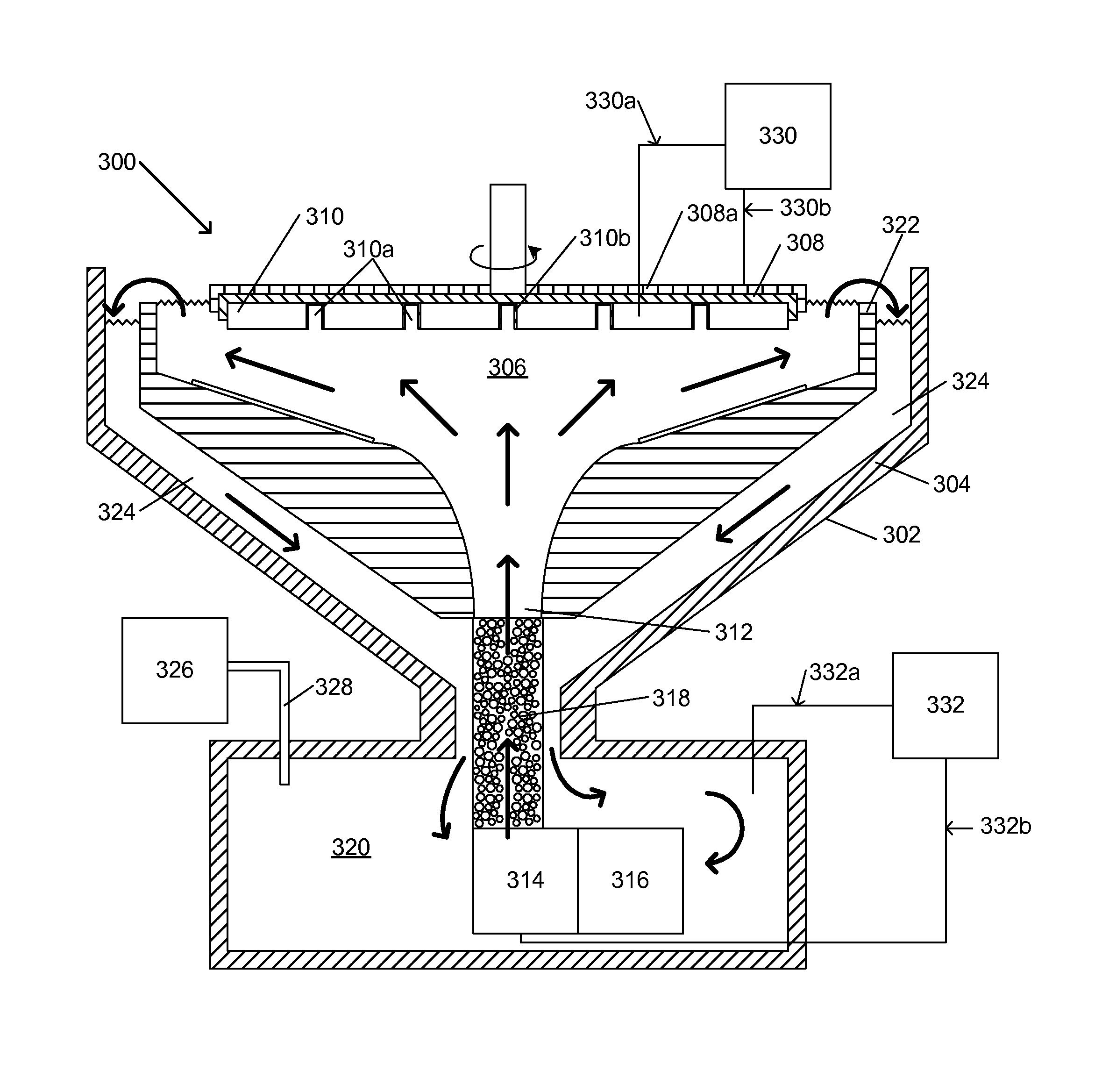
[0202]To produce a TSV filled with a high purity copper deposit, a wafer is provided with vias having a diameter of about 10 microns and a depth of about 50 microns. The inner sidewalls of the vias are coated with a diffusion barrier layer formed from tantalum nitride applied by sputtering. The tantalum nitride layer is covered with a liner layer of tantalum applied by sputtering. Next, the liner layer is coated with a copper basic metal layer by sputtering, in which the copper basic metal layer has a thickness of about 0.1 micron. The wafer is then immersed in a copper deposition bath described below in which the wafer is connected as a cathode, heated to about 40° C., an insoluble anode is included in the apparatus, and the bath is maintained at room temperature. The via is filled with high purity copper by electrodeposition from the bath having the following ingredients, to form the TSVs in accordance with the present invention:

H2SO4, 98% by wt.130g / lCuSO4•5 H2O70g / lFeSO4•7 H2O15...

example 2

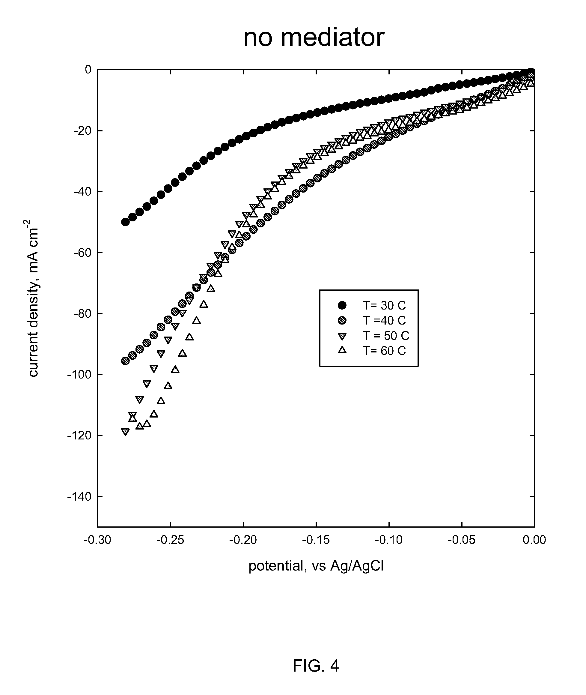
[0208]Copper stress in TSVs deposited by different plating methods using the bath of Example 1, in accordance with the invention, including heating the wafer substrate and maintaining the bath at the lower temperature, and in a first comparative example, using a similar bath and a soluble copper anode without the added Fe2+ / Fe3+ ions and without heating the wafer substrate and in a second comparative example using a similar bath including all the above ingredients but without heating the wafer substrate, in which pulsed current is applied with the parameters shown in the table below:

Pulse inmillisecondsPhaseIforward / IreverseForward- / Pulse-gap inshift inExamplesin A / dm2Reverse-Pulsemillisecondsdegrees1 and 26 / 4072 / 44180

Electrodeposition MethodStressCu RateUnheated wafer, soluble copper anode:163.2 ± 34.3 MPa(prior art)Unheated wafer w / Cu / Cu2+ / Fe2+ / Fe3+113.4 ± 40.1 MPa≈1 μ / minredox (prior art)Heated wafer w / Cu / Cu2+ / Fe2+ / Fe3+ redox66.9 ± 9.8 MPa≈2 μ / min(present invention)

[0209]The inte...


PUM

PropertyMeasurementUnit
Temperatureaaaaaaaaaa

Abstract

Process of electrodepositing a metal in a high aspect ratio via in a silicon substrate to form a through-silicon-via (TSV), utilizing an electrolytic bath including a redox mediator, in an electrolytic metal plating system including a chuck adapted to hold the silicon substrate and to heat the silicon substrate to a first temperature, a temperature control device to maintain temperature of the electrolytic bath at a second temperature, in which the first temperature is maintained in a range from about 30° C. to about 60° C. and the second temperature is maintained at a temperature (a) at least 5° C. lower than the first temperature and (b) in a range from about 15° C. to about 35° C.

Description

BACKGROUND[0001]1. Field of the Invention[0002]The invention relates to a process of electrolytically forming conductor structures from highly pure copper, more specifically to electrolytically forming conductor structures from highly pure copper in through-silicon vias (TSVs) when producing devices such as MEMS or semiconductor devices. Such TSVs are useful, e.g., in integrated circuits, in a stacked or 3D arrangement, in which the TSV provide electrical connection between the respective layers of the device, where the TSV have relatively large diameter, relatively great depth and a high aspect ratio. The electrolytic formation of conductor structures is enhanced and improved by application of heat to the substrate while maintaining the electrolytic bath at a lower temperature.[0003]2. Description of Related Art[0004]The demands of fabricating cheaper, smaller and lighter electronic products offering better performance and increased functionality are continuously growing. The numbe...

Claims


Application Information

Patent Timeline
IPC IPC(8): H01L21/445
CPCC25D3/38C25D5/00C25D21/02H01L21/2885H01L21/76898H01L25/50C25D7/123H01L2225/06541H01L2224/73204H01L2225/06513H01L2924/1461C25D17/001H01L2224/16225H01L2224/32225H01L2924/00012H01L2224/16145H01L2224/32145H01L2924/00H01L2224/131H01L2924/014C25D7/12H01L21/288
Inventor PREISSER, ROBERT F.
Owner ATOTECH DEUT GMBH
Why Eureka
Try Eureka