GeSn Infrared Photodetectors

a technology of infrared photodetectors and infrared light, which is applied in the field of infrared light detectors, can solve the problems of compromising the compatibility with cmos technology, increasing the thermal budget, and drastically reducing the responsivity of ir detection, so as to increase the optical absorption, increase the quantum efficiency, and expand the range of ir detection.

Inactive Publication Date: 2012-02-02
ARIZONA STATE UNIVERSITY
View PDF2 Cites 45 Cited by
  • Summary
  • Abstract
  • Description
  • Claims
  • Application Information

AI Technical Summary

Benefits of technology

[0006]It has been found that even minor amounts of Sn incorporation (2%) can dramatically expand the range of IR detection up to at least 1750 nm, well below the direct bandgap of Ge (1550 nm), and substantially increase the optical absorption. The corresponding photoresponse can yield higher quantum efficiencies than comparable pure-Ge devices over a broader spectrum, allowing coverage of all telecommunication bands using entirely group IV materials.

Problems solved by technology

This is a challenging task due to the inferior crystalline quality and high dislocation densities in Ge / Si layers resulting from the 4% lattice mismatch between the two materials.
Unfortunately, even pure Ge is only marginally acceptable as a near infrared detector, since its direct absorption edge at 1550 nm is in the middle of the “erbium window” (C-band), and its responsivity is drastically reduced at wavelengths corresponding to the L- and U-telecommunication windows, for which only indirect gap absorption is possible.
However, this approach increases the thermal budget, compromising the compatibility with CMOS technology, and still fails to fully cover the L- and U-bands.

Method used


Image

  • GeSn Infrared Photodetectors
  • GeSn Infrared Photodetectors
  • GeSn Infrared Photodetectors

Examples


example 1

Optoelectronic Ge1-ySny Alloys

[0146]From a fundamental view point Ge1-ySny alloys on their own right are intriguing IR materials that undergo an indirect-to-direct band gap transition with variation of their strain state and / or compositions. They also serve as versatile, compliant buffers for the growth of II-VI and III-V compounds on Si substrates.

[0147]The fabrication of the Ge1-ySny materials directly on Si wafers has recently been reported using a specially developed CVD method involving reactions of Ge2H6 with SnD4 in high purity H2 (10%). Thick and atomically flat films are grown at about 250 to about 350° C. and possess low densities of threading dislocations (˜105 cm−2) and high concentrations of Sn atoms up to about 20%. Since the incorporation of Sn lowers the absorption edges of Ge, the Ge1-ySny alloys are attractive for detector applications that require band gaps lower than that of Ge (0.80 eV). The absorption coefficient of selected Ge1-xSnx samples, showing high absor...

example 2

Fabrication of Ge1-xSnx Infrared Detector

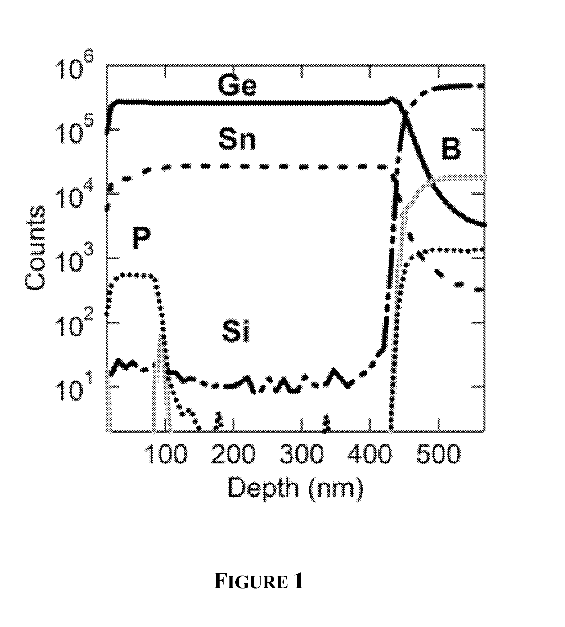
[0150]Ge0.98Sn0.02 active material was grown on boron-doped (p-type) Si(100) with resistivity 0.01 Ωcm. Prior to growth, the wafers were chemically cleaned by a modified RCA process and then dipped in 5% HF solution to hydrogen-passivate their surface. The UHV-CVD growth of the intrinsic Ge0.98Sn0.02 was conducted by reactions of digermane Ge2H6 and deuterated stannane SnD4 at 350° C. and 300 mTorr, yielding an average growth rate of about 10 nm / min. A post growth annealing step, consisting of 3 cycles at 750° C. for 2 seconds, was used to reduce the levels of threading defects and ensure that the material is devoid of any residual strains. The wafers were then loaded back into the growth chamber to conduct the deposition of the n-type capping layer using a 1% admixture P(GeH3)3 as the source of the P atoms. This compound and related families of single source dopants [(P,As)(MH3)3, M=Si,Ge] are the key enabling ingredient for low-temperature ...

example 3

Fabrication of Ge1-xSnx Infrared Detector

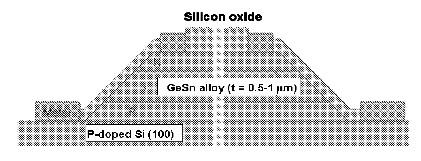
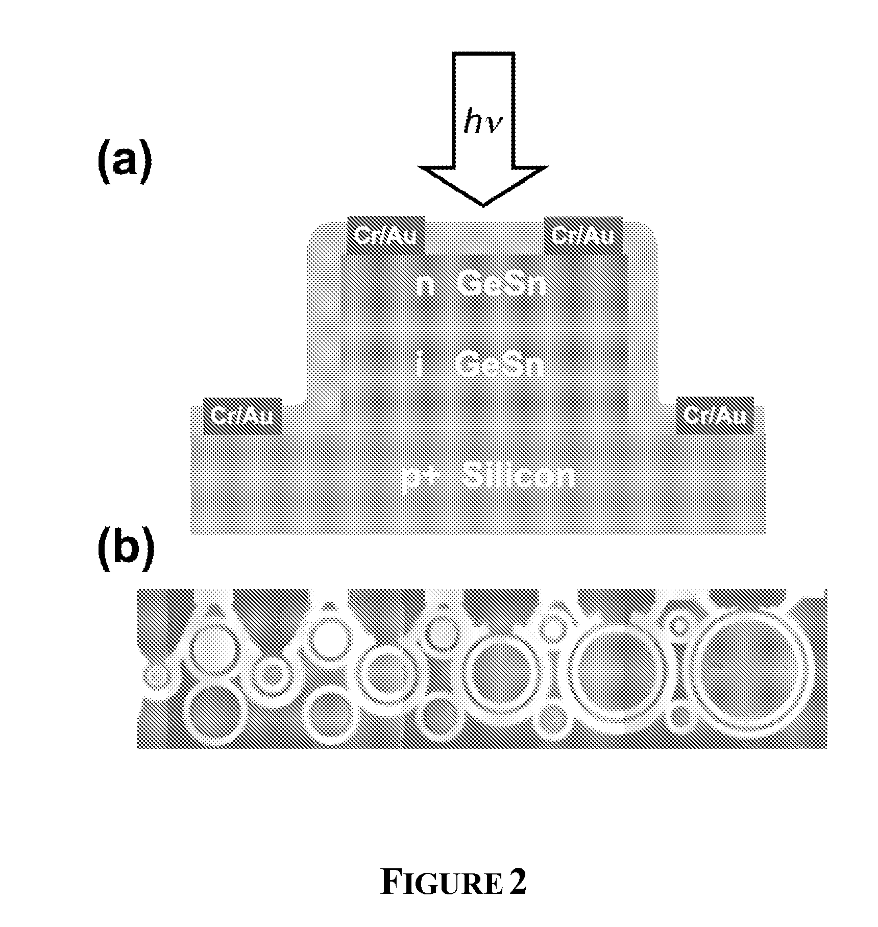
[0156]A infrared detector was fabricated as illustrated in cross-section in FIG. 6 comprising Ge1-xSnx pin regions on a p-doped Si substrate. The preliminary test results indicated that the fabricated PIN devices show diode I-V characteristics and also exhibit significant IR photoresponse at 1.55 μm. In these devices and the related photoconductor counterparts, linear, ohmic contacts were readily demonstrated on top of the n-type Ge1-xSnx layers indicating that successful high doping of these Ge-rich semiconductors is achievable using hydride precursors developed at ASU. The in situ protocols described above using gaseous As(GeH3)3 reactants enable facile incorporation of the As atoms into the lattice at low growth temperatures of 350° C., and promote full activation of the entire dopant concentration (˜1018 cm−3-1020 cm−3).

[0157]The newly developed Ge1-xSnx photodetector and photoconductor structures are attractive devices in their own right...


PUM


Abstract

Photodiode devices with GeSn active layers can be integrated directly on p+ Si platforms under CMOS-compatible conditions. It has been found that even minor amounts of Sn incorporation (2%) dramatically expand the range of IR detection up to at least 1750 nm and substantially increases the absorption. The corresponding photoresponse can cover of all telecommunication bands using entirely group IV materials.

Description

CROSS-REFERENCE TO RELATED APPLICATIONS[0001]This application claims the benefit of the filing date of U.S. Provisional Application Ser. No. 61 / 097,272, filed Sep. 16, 2008, and U.S. Provisional Application Ser. No. 61 / 105,670, filed Oct. 15, 2008, each of which is hereby incorporated by reference in their entirety.STATEMENT OF GOVERNMENT FUNDING[0002]The invention described herein was made in part with government support under grant number DEFG3608GO18003, awarded by the Department of Energy; and grant number FA9550-06-01-0442 awarded by the United States Air Force Office of Scientific Research (AFOSR). The United States Government has certain rights in the invention.FIELD OF THE INVENTION[0003]The invention generally relates to infrared photodetectors comprising Group IV semiconductor layers.BACKGROUND OF THE INVENTION[0004]The application of silicon photonic technologies to optical telecommunications requires the development of near-infrared detectors monolithically integrated to...

Claims


Application Information

Patent Timeline
Patent Type & Authority Applications(United States)
IPC IPC(8): H01L33/02H01L31/107H01L31/18H01L31/102
CPCH01L21/02381H01L21/0245H01L21/02452H01L21/02532H01L31/107H01L21/0257H01L27/14649H01L31/03125H01L31/075H01L21/02535
Inventor KOUVETAKIS, JOHNMENENDEZ, JOSEROUCKA, RADEKMATHEWS, JAY
Owner ARIZONA STATE UNIVERSITY
Why Eureka
Try Eureka