Manufacturing methods of thin film transistor, liquid crystal display device, and semiconductor device

a technology of liquid crystal display device and thin film transistor, which is applied in the direction of semiconductor devices, electrical appliances, basic electric elements, etc., can solve the problems of reducing the yield, and achieve the effect of reducing the manufacturing steps of the liquid crystal display device, high productivity and low cos

Inactive Publication Date: 2012-03-01
SEMICON ENERGY LAB CO LTD
View PDF6 Cites 54 Cited by
  • Summary
  • Abstract
  • Description
  • Claims
  • Application Information

AI Technical Summary

Benefits of technology

[0027]According to one embodiment of the present invention, manufacturing steps of a liquid crystal display device can be significantly reduced, whereby a liquid crystal display device can be provided with high productivity at low cost.
[0028]A liquid crystal display device with less power consumption and high reliability can be provided.

Problems solved by technology

There is a possibility that the yield is decreased due to various problems caused by usage of such a complicated technique.

Method used


Image

  • Manufacturing methods of thin film transistor, liquid crystal display device, and semiconductor device
  • Manufacturing methods of thin film transistor, liquid crystal display device, and semiconductor device
  • Manufacturing methods of thin film transistor, liquid crystal display device, and semiconductor device

Examples


embodiment 1

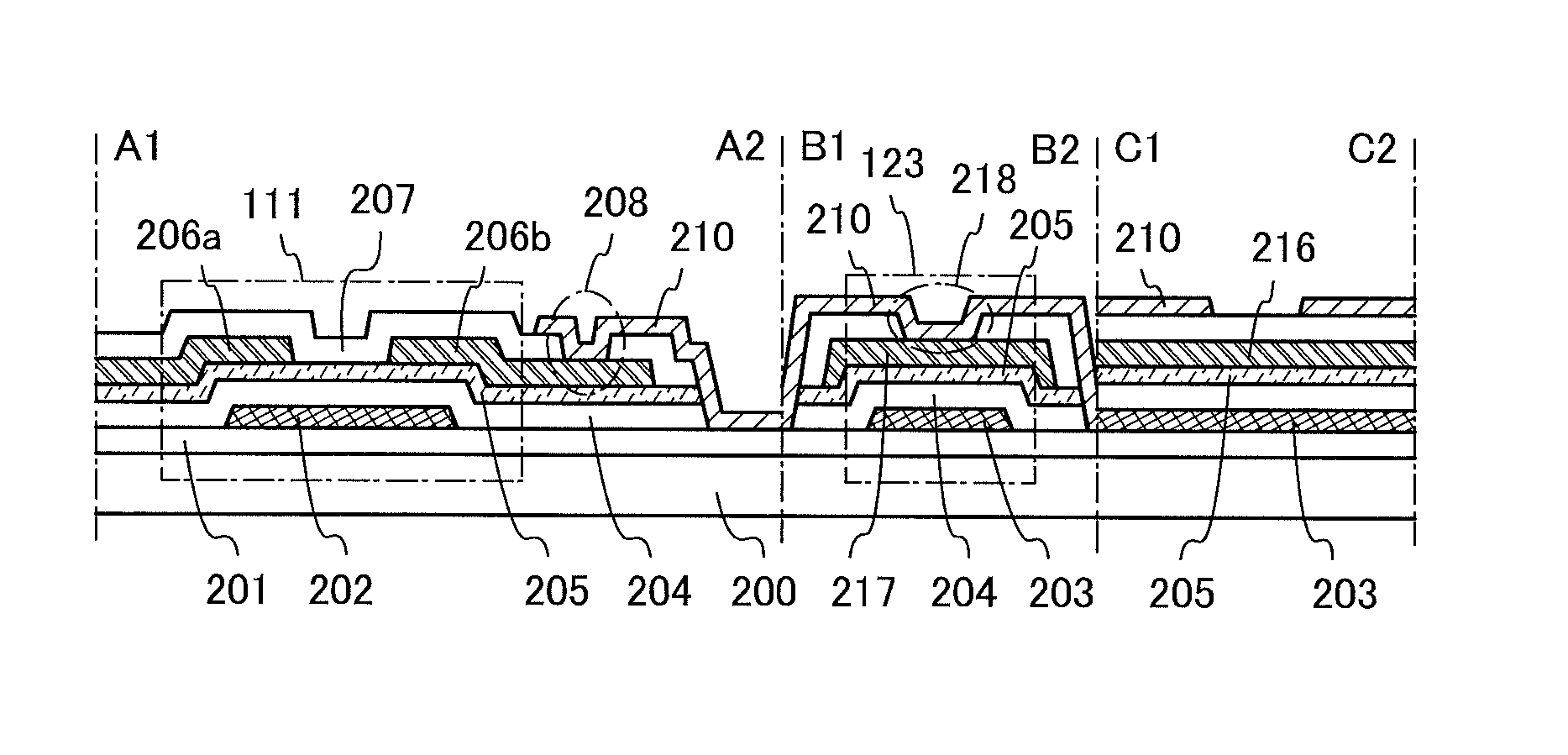
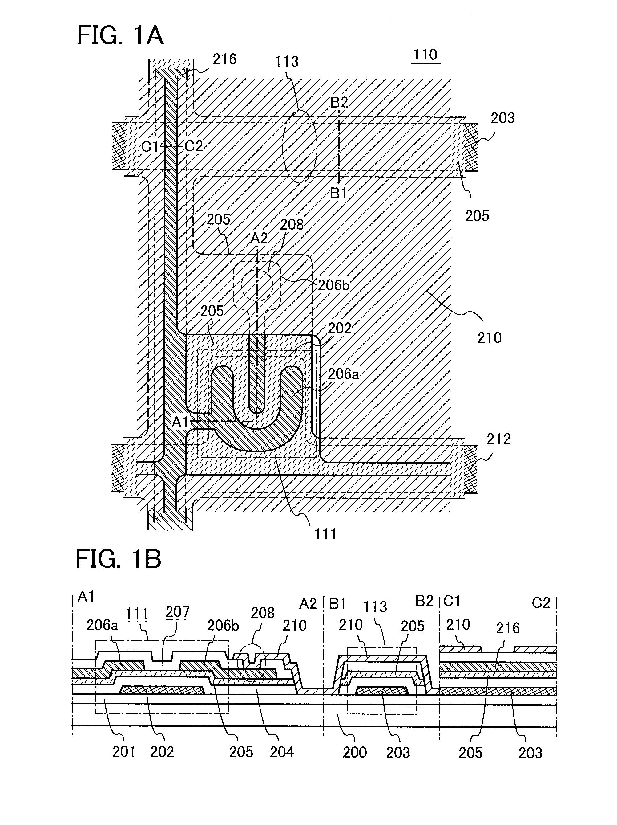
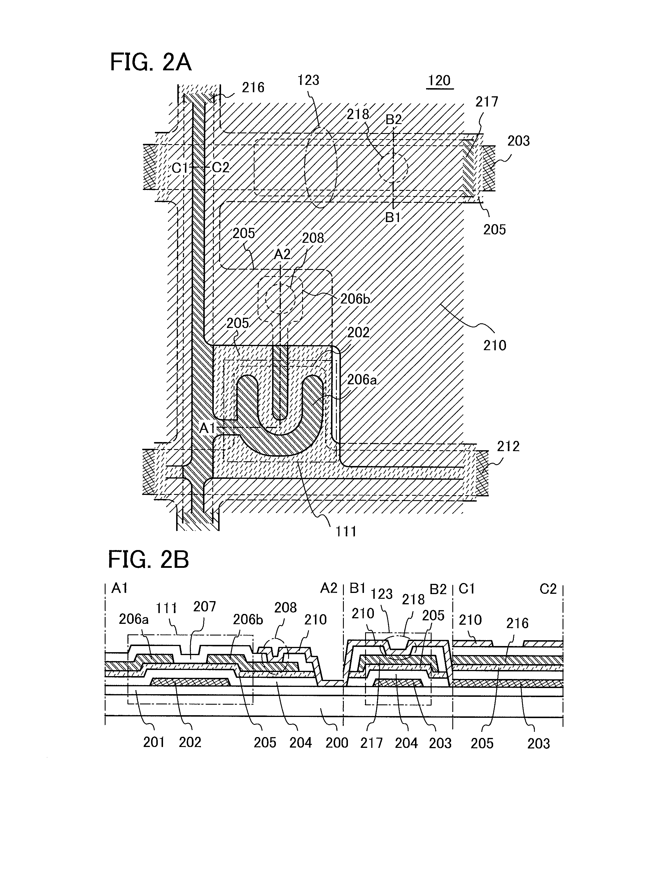
[0048]In this embodiment, as examples, pixel structures and a manufacturing method of liquid crystal display devices for which a reduced number of photomasks and a reduced number of photolithography processes are reduced are described with reference to FIGS. 1A and 1B, FIGS. 2A and 2B, FIGS. 3A and 3B, FIGS. 4A-1, 4A-2, 4B-1, and 4B-2, FIGS. 5A to 5C, and FIGS. 6A to 6C.

[0049]FIG. 3A shows a structure example of a semiconductor device 100 used in a liquid crystal display device. The semiconductor device 100 includes, over a substrate 101, a pixel region 102, a terminal portion 103 including in (m is an integer greater than or equal to 1) terminals 105, and a terminal portion 104 including n (n is an integer greater than or equal to 1) terminals 106. The semiconductor device 100 also includes m wirings 212 electrically connected to the terminal portion 103, and n wirings 216 electrically connected to the terminal portion 104. The pixel region 102 includes a plurality of pixels 110 ar...

embodiment 2

[0176]In this embodiment, a process example partly different from that described in Embodiment 1 is described with reference to FIGS. 7A to 7C. Note that the same reference numerals are used for the same parts as those in Embodiment 1, and description of the parts with the same reference numerals is omitted here.

[0177]First, as in Embodiment 1, a conductive layer is formed over the substrate 200 having an insulating surface, and then, the gate electrode 202 is formed through the first photolithography process and an etching step.

[0178]An insulating layer serving as a base layer may be formed between the substrate 200 and the gate electrode 202. In this embodiment, the base layer 201 is formed. The base layer 201 has a function of preventing diffusion of an impurity element (e.g., Na) from the substrate 200, and can be formed using a film selected from a silicon oxide film, a silicon oxynitride film, a silicon nitride film, a hafnium oxide film, an aluminum oxide film, a gallium oxid...

embodiment 3

[0189]One mode of a display device including the transistor described in Embodiment 1 and Embodiment 2 is illustrated in FIGS. 8A and 8B.

[0190]FIG. 8A is a plan view of a panel in which a transistor 4010 and a liquid crystal element 4013 are sealed between a first substrate 4001 and a second substrate 4006 with a sealant 4005. FIG. 8B is a cross-sectional view taken along line M-N in FIG. 8A.

[0191]The sealant 4005 is provided so as to surround a pixel portion 4002 provided over the first substrate 4001, and the second substrate 4006 is provided over the pixel portion 4002. Accordingly, the pixel portion 4002 is sealed together with a liquid crystal layer 4008 by the first substrate 4001, the sealant 4005, and the second substrate 4006.

[0192]An input terminal 4020 is provided in a region that is different from the region surrounded by the sealant 4005 over the first substrate 4001. Flexible printed circuits (FPCs) 4018a and 4018b are connected to the input terminal 4020. The FPC 4018...


PUM


Abstract

A liquid crystal display device is provided with high productivity at low cost by reducing manufacturing steps of the liquid crystal display device. A liquid crystal display device with less power consumption and high reliability is provided. Etching of a semiconductor layer and formation of a contact hole that connects a pixel electrode and a drain electrode are performed by one photolithography process and one etching step, whereby the number of photolithography processes is reduced. A liquid crystal display device can be provided with high productivity at low cost by reducing the number of photolithography processes. Further, an oxide semiconductor is used for the semiconductor layer, whereby a liquid crystal display device with less power consumption and high reliability can be provided.

Description

BACKGROUND OF THE INVENTION[0001]1. Field of the Invention[0002]The present invention relates to manufacturing methods of a thin film transistor, a liquid crystal display device, and a semiconductor device.[0003]In this specification, a semiconductor device means all types of devices which can function by utilizing semiconductor characteristics, and a semiconductor circuit, a memory device, an imaging device, a display device, an electro-optical device, an electronic device, and the like are all semiconductor devices.[0004]2. Description of the Related Art[0005]In recent years, thin film transistors that are formed using a semiconductor thin film having a thickness of several nanometers to several hundreds of nanometers over a substrate having an insulating surface such as a glass substrate have been attracting attentions. Thin film transistors are widely used for electronic devices such as integrated circuits (ICs) and electro-optical devices. In particular, thin film transistors a...

Claims


Application Information

Patent Timeline
Patent Type & Authority Applications(United States)
IPC IPC(8): H01L21/428
CPCH01L27/1214H01L29/41733H01L27/1225H01L27/1255H01L27/1288
Inventor YAMAZAKI, SHUNPEI
Owner SEMICON ENERGY LAB CO LTD
Why Eureka
Try Eureka