Electrical switch using gated resistor structures and three-dimensional integrated circuits using the same

a gated resistor and integrated circuit technology, applied in the direction of semiconductor devices, electrical apparatus, transistors, etc., can solve the problems of significant processing modifications, limited tsv dimensions, and significant limitations on the feasibility of monolithic stacking, and achieve low thermal budget and high interconnect density.

Active Publication Date: 2012-03-08
CHEN SHU LU
View PDF9 Cites 25 Cited by
  • Summary
  • Abstract
  • Description
  • Claims
  • Application Information

AI Technical Summary

Benefits of technology

[0015]It is an object of the present invention to provide a new methodology and structure for 3D integration with low thermal budget and high interconnect density.

Problems solved by technology

The dimension of TSV is limited by the ability of high aspect ratio etching and the alignment accuracy during bonding.
However, monolithic stacking involves significant processing modifications for the layer that fabricated on top of the existing layer.
Such thermal constrains poses significant limitation on the feasibility of monolithic stacking.
For monolithic stacking, despite its potential ability of providing high interconnect density, the difficulty in fabrication, particularly thermal budget, limits its adoption.
There are, however, two high temperature critical steps limit the feasibility of monolithic stacking integration: getting a high quality single crystal substrate on top of existing layer / devices, and subsequent dopant activation.
The activation of source / drain (S / D) in current Si technology often requires temperature much higher than 450° C., and low temperature source / drain annealing results in significant performance loss and high contact resistance.
Laser annealing has been pursued because the energy can be limited locally, but such process generally has lower throughput.
Aside from dopant activation, getting a single crystal substrate to start with is also problematic because it is hard to form single crystal layer on top of the amorphous isolation layer, which encapsulates the devices in the lower layer.
However, source / drain regions activation is more problematic since traditionally they are done after fine pitch gate patterning.
As a result, if the fine pitch gate module and S / D anneal are done before bonding, then the whole approach actually becomes the previous mentioned wafer bonding technique which still suffers from the possibility of misalignment during bonding.

Method used


Image

  • Electrical switch using gated resistor structures and three-dimensional integrated circuits using the same
  • Electrical switch using gated resistor structures and three-dimensional integrated circuits using the same
  • Electrical switch using gated resistor structures and three-dimensional integrated circuits using the same

Examples


Embodiment Construction

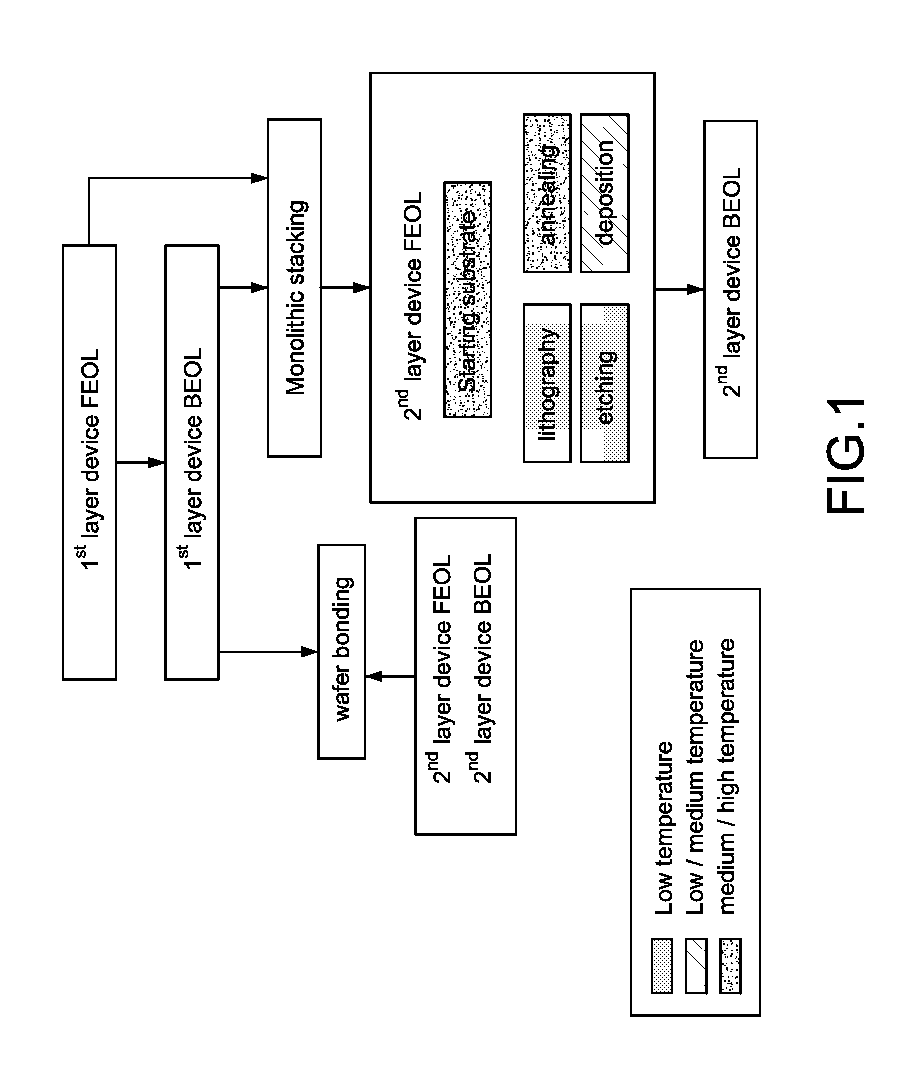
[0042]BSMC Methodology

[0043]To resolve the issues arising from TSV / wafer bonding and monolithic stacking, a “bonding substrate / monolithic contact” (BSMC) methodology for multiple layer device fabrication is proposed and illustrated in FIG. 3. The general concept is that since substrate annealing and channel activation do not require accurate alignment to the previous layer, they should be done before bonding to avoid unnecessary thermal impact to the acceptor wafer. By doing so we essentially eliminate one of the two thermal bottlenecks mentioned above, leaving only the S / D dopant annealing. For example, we could start with a regular Si substrate, implant and activated, then transferred to an acceptor wafer using oxide to oxide bonding. The bonding process requires little effort on the alignment since at this moment, the layers (implanted and activated) being transferred do not have any fine pitch patterns defined. After the transfer, similar process flow sequence for fabricating a ...


PUM


Abstract

An electrical switch using a gated resistor structure includes an isolation layer, a doped silicon layer arranged on the isolation layer and having a recessed portion with reduced thickness, the doped silicon layer having a predetermined doping type and a predetermined doping profile; a gate layer arranged corresponding to the recessed portion. The recessed portion in the doped silicon layer has such thickness that a channel defined under the gate can be fully depleted to form a high resistivity region. The recessed channel gated resistor structure can be advantageously used to achieve high interconnect density with low thermal budget for 3D integration.

Description

CROSS-REFERENCE TO RELATED APPLICATIONS[0001]This application claims priority benefit of U.S. Provisional Patent Application No. 61 / 380,283, filed on Sep. 6, 2010 and entitled “Process and structure for three-dimensional integrated circuit by transferred substrate and gated resistor,” which is hereby incorporated herein by reference.BACKGROUND OF THE INVENTION[0002]1. Field of the Invention[0003]The present invention relates to low thermal budget gated resistor structures, and more particularly, its application for device level three-dimensional (3D) integration with higher interconnect density compared to the current wafer bonding / packaging and “through silicon via” (TSV) technology.[0004]2. Description of the Related Art[0005]In response to the increasing challenges in maintaining technology advancements through traditional “constant electrical field” scaling at a pace consistent with Moore's law, alternative methods to achieve enhanced system level performance are becoming increa...

Claims


Application Information

Patent Timeline
Patent Type & Authority Applications(United States)
IPC IPC(8): H01L29/788H01L21/336H01L29/78
CPCH01L21/76254H01L21/823807H01L21/823828H01L27/0688H01L29/66621H01L2924/0002H01L29/7838H01L29/78654H01L2924/00Y02P80/30
Inventor CHEN, SHU-LU
Owner CHEN SHU LU
Why Eureka
Try Eureka