Method for manufacturing semiconductor device

a semiconductor film and film technology, applied in the direction of semiconductor devices, electrical equipment, basic electric elements, etc., can solve the problems of significant impairing of threshold voltage of transistor reliability, and achieve the effects of stable electrical characteristics, less variation in threshold voltage, and reduced hydrogen contained in oxide semiconductor films

Inactive Publication Date: 2012-03-08
SEMICON ENERGY LAB CO LTD
View PDF0 Cites 56 Cited by
  • Summary
  • Abstract
  • Description
  • Claims
  • Application Information

AI Technical Summary

Benefits of technology

[0017]According to one embodiment of the present invention, hydrogen contained in an oxide semiconductor film can be reduced, and a transistor having stable electrical characteristics with less variation in threshold voltage can be provided.
[0018]Alternatively, according to one embodiment of the present invention, hydrogen in a film in contact with an oxide semiconductor film can be reduced, and thus entry of hydrogen into the oxide semiconductor film can be suppressed. Consequently, a semiconductor device having a transistor with favorable electrical characteristics and high reliability can be provided.

Problems solved by technology

A change in the threshold voltage significantly impairs the reliability of the transistor.

Method used


Image

  • Method for manufacturing semiconductor device
  • Method for manufacturing semiconductor device
  • Method for manufacturing semiconductor device

Examples


embodiment 1

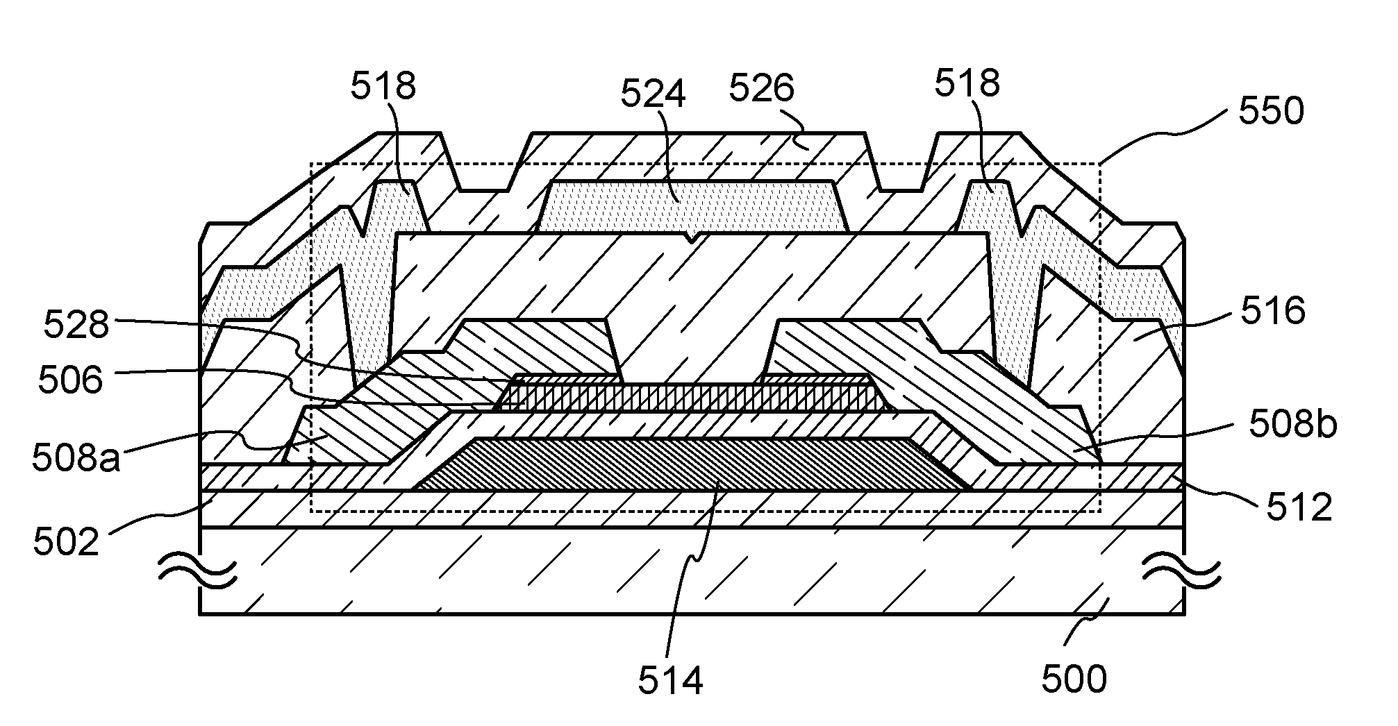
[0038]In this embodiment, description is made on a method for manufacturing a top-gate top-contact transistor using an oxide semiconductor with less entry of hydrogen into a film and an interface between films.

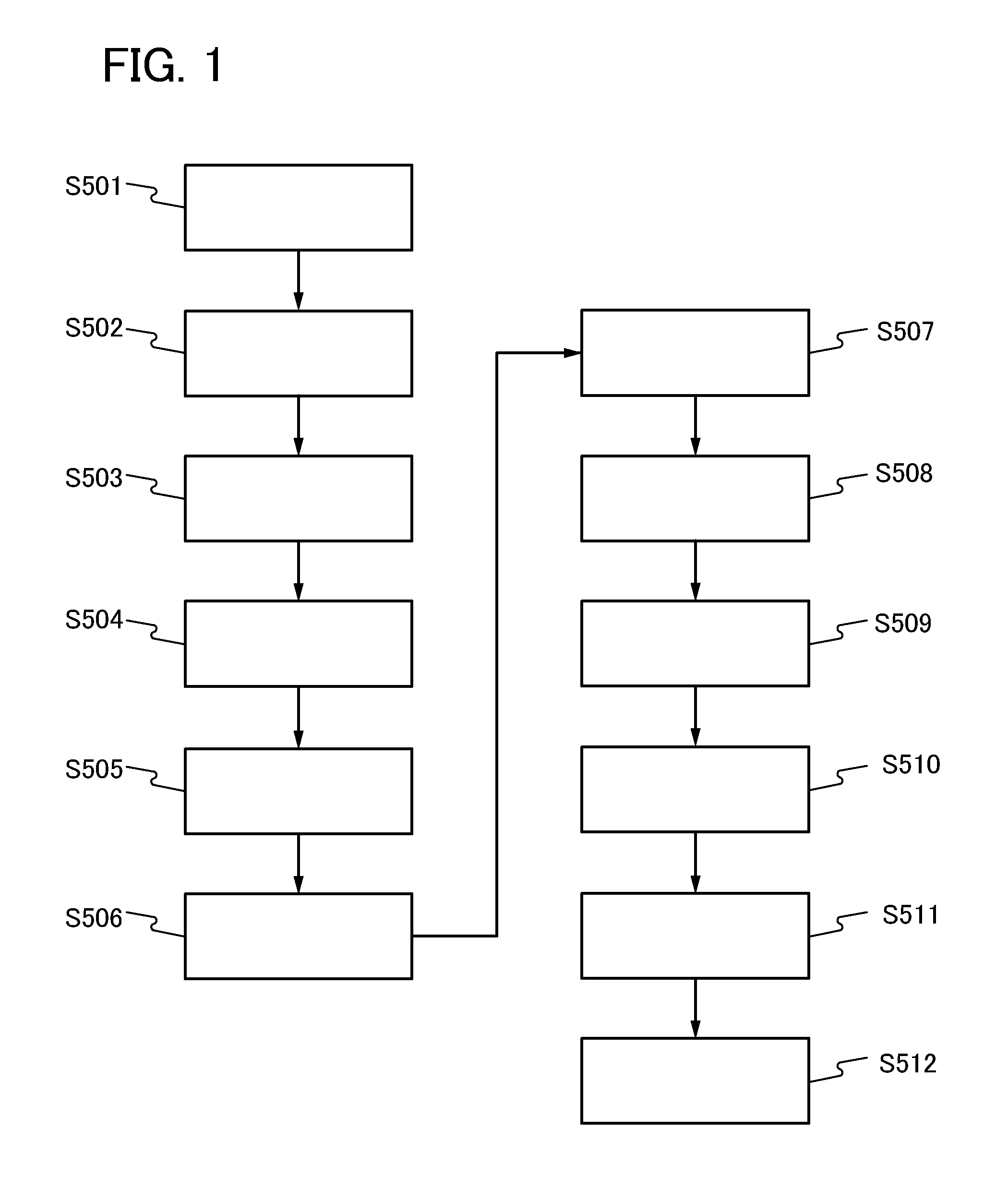
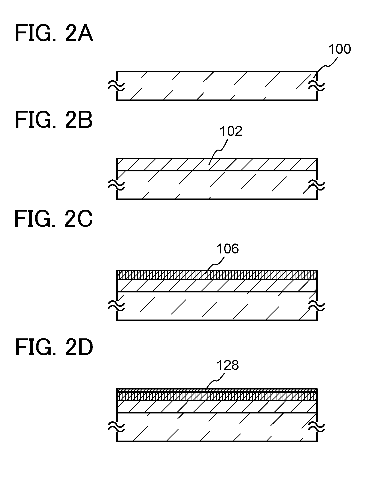
[0039]FIG. 1 is a flow chart showing a path of a substrate in a multi-chamber film formation apparatus. FIGS. 2A to 2D are cross-sectional views that shows a method for manufacturing a semiconductor device and corresponds to the flow diagram in FIG. 1.

[0040]FIG. 3 is a multi-chamber film formation apparatus. The film formation apparatus includes a substrate supply chamber 11 having three cassette ports 14 accommodating a substrate, a load lock chamber 12a, a load lock chamber 12b, a transfer chamber 13, a substrate processing chamber 15, a film formation chamber 10a with a leakage rate less than or equal to 1×10⁻¹⁰ Pa·m3 / sec, a film formation chamber 10b with a leakage rate less than or equal to 1×100 Pa·m3 / sec, and a film formation chamber 10c with a leakage rate less than or...

embodiment 2

[0103]In this embodiment, description is made on a method for manufacturing a bottom-gate top-contact transistor using an oxide semiconductor with less entry of hydrogen into a film and an interface between films.

[0104]FIG. 6 is a flow chart showing a path of a substrate in a multi-chamber film formation apparatus. FIGS. 7A to 7C are cross-sectional views corresponding to a manufacturing flow in FIG. 6. A multi-chamber film formation apparatus similar to that in Embodiment 1 is used.

[0105]First, as shown in a step S601 in FIG. 6, a substrate 200 is put on the cassette port 14 in the substrate supply chamber 11.

[0106]Next, as shown in a step S602 in FIG. 6, the gate valve of the load lock chamber 12a set to an atmospheric pressure state is opened, the substrate 200 is transferred from the cassette port 14 to the load lock chamber 12a with the first transfer robot, and then the gate valve is closed.

[0107]The load lock chamber 12a is evacuated and set to a vacuum state after the substr...

embodiment 3

[0137]In this embodiment, description is made on a method for manufacturing a bottom-gate top-contact transistor using an oxide semiconductor with less entry of hydrogen into a film and an interface between films with reference to FIGS. 10A to 10E. The method is different from that in Embodiment 2. Note that steps up to and including those in the flow of FIG. 6 and FIGS. 7A to 7C are similar to those in Embodiment 2.

[0138]Manufacturing steps up to and including those in FIGS. 10A and 10B are similar to those in the manufacturing steps up to and including those in FIGS. 8A and 8B.

[0139]After the oxide semiconductor film 206 is formed, the substrate 200 is subjected to heat treatment or plasma treatment. By subjecting the oxide semiconductor film 206 to the heat treatment or the plasma treatment, the oxide semiconductor film 206 can be dehydrated or dehydrogenated. The heat treatment or the plasma treatment is performed at a temperature higher than or equal to 150° C. and lower than t...


PUM


Abstract

Electrical characteristics of transistors using an oxide semiconductor are greatly varied in a substrate, between substrates, and between lots, and the electrical characteristics are changed due to heat, bias, light, or the like in some cases. In view of the above, a semiconductor device using an oxide semiconductor with high reliability and small variation in electrical characteristics is manufactured. In a method for manufacturing a semiconductor device, hydrogen in a film and at an interface between films is removed in a transistor using an oxide semiconductor. In order to remove hydrogen at the interface between the films, the substrate is transferred under a vacuum between film formations. Further, as for a substrate having a surface exposed to the air, hydrogen on the surface of the substrate may be removed by heat treatment or plasma treatment.

Description

TECHNICAL FIELD[0001]The present invention relates to a film formation apparatus and a method for manufacturing a semiconductor device using the film formation apparatus.[0002]Note that in this specification, a semiconductor device refers to any device that can function by utilizing semiconductor characteristics, and an electro-optical device, a semiconductor circuit, and an electronic device are all semiconductor devices.BACKGROUND ART[0003]In recent years, attention has been focused on a technique for forming transistors using semiconductor thin films formed over a substrate having an insulating surface. The transistors are applied to a wide range of electronic devices such as an integrated circuit (IC) or an image display device (display device). As materials of semiconductor thin films applicable to the transistors, silicon-based semiconductor materials have been widely known, but oxide semiconductors have been attracting attention as alternative materials.[0004]For example, dis...

Claims


Application Information

Patent Timeline
Patent Type & Authority Applications(United States)
IPC IPC(8): H01L21/34
CPCH01L21/02554H01L21/02565H01L21/02631H01L21/02488H01L29/7869H01L29/66969H01L29/78603H01L21/283
Inventor YAMAZAKI, SHUNPEI
Owner SEMICON ENERGY LAB CO LTD
Why Eureka
Try Eureka