Modified nano-dot, fabrication method thereof and composition element thereof

a technology of nano-dot and composition element, which is applied in the direction of electroluminescent light sources, chemistry apparatus and processes, and compositions. it can solve the problems of low electroluminescence efficiency, low efficiency devices, and limited practical applicability, so as to achieve favorable use, bright emission, and high surface charge

Inactive Publication Date: 2012-03-15
NATIONAL TSING HUA UNIVERSITY
View PDF4 Cites 0 Cited by
  • Summary
  • Abstract
  • Description
  • Claims
  • Application Information

AI Technical Summary

Benefits of technology

[0007]In consideration of the above problems of the prior art, it is an objective of the present invention to provide a modified nano-dot capable of significantly enhancing the efficiency of organic electronic elements, such as organic light emitting diodes, organic solar cells and the like. The modified nano-dot comprises two main portions: a surface portion which may comprise a functional group, such as an amino group, a hydroxyl group, an alkyl group, an alkenyl group, a halogen group or a phosphite group; and a core portion which may comprise a polymeric metal, metalloid or metal alloy oxide. The polymeric metal oxide may comprise an oxide of aluminum, tin, magnesium, calcium, titanium, manganese, zinc, gold, silver, copper, nickel or iron. The metalloid of the polymeric metalloid oxide may comprise silicon. The mean particle size of the modified nano-dot is 1-100 nm, preferably 1-10 nm. Furthermore, the modified nano-dot possesses a high surface charge comprising a positive charge of +1 to +200 mV or a negative charge of −1 to −200 mV.
[0009]According to the objective of the present invention, a composition element with a modified nano-dot is provided. The nano-dot is capable of effectively modulating a carrier flux and can be applied to, for example, the organic semiconductor industry, optoelectronics industry, and solar cell industry.
[0010]As described above, the modified nano-dot and the fabrication method thereof may have one or more following advantages:
[0012](2) The modified nano-dots according to the present invention are prepared in a solution state so that they can be directly applied to the elements by wet-process. This enables the modified nano-dots to be homogeneously distributed in an element.
[0013](3) The modified nano-dots according to the present invention can possess high surface charges so that they can be favorably used in the organic semiconductor industry, optoelectronics industry, and solar cell industry. For example, in the application of organic light emitting diodes, the high surface positive or negative charges of the modified nano-dots can effectively modulate the transporting flux of the carriers via blocking or trapping mechanism. This can effectively prevent the holes from entering the emissive layer and causing imbalanced carrier-injection. Furthermore, in the presence of high repelling or dragging field arising from the highly charged nano-dots, only holes with high energy are able to succeed in passing over the barriers wherein, which in turn causes them to penetrate thereafter deeper into the emissive layer, leading carrier recombination to take place in a wider region, resulting in a brighter emission and hence a higher power-efficiency.

Problems solved by technology

Previous studies at depositing quantum-dots into an emissive layer or incorporating nano-dots in a non-emissive layer of an organic light emitting diode have shown significant efficiency improvement, but only for low-efficiency devices.
However, no report has yet revealed these approaches to be effective as well on high-efficiency devices, seriously limiting their practical applicability.
The low electroluminescence (EL) efficiency may be attributed to a number of causes, comprising high carrier-injection-barrier, low carrier- and exciton-confinement, excitons forming on a guest, poor energy-transfer efficiency, intrinsically low material electroluminescence, and, most critically, imbalanced carrier-injection, etc.
However, the overall efficiency is still low even though the relative improvement is strikingly sound (still less than 25 lm / W).

Method used


Image

  • Modified nano-dot, fabrication method thereof and composition element thereof
  • Modified nano-dot, fabrication method thereof and composition element thereof
  • Modified nano-dot, fabrication method thereof and composition element thereof

Examples


Embodiment Construction

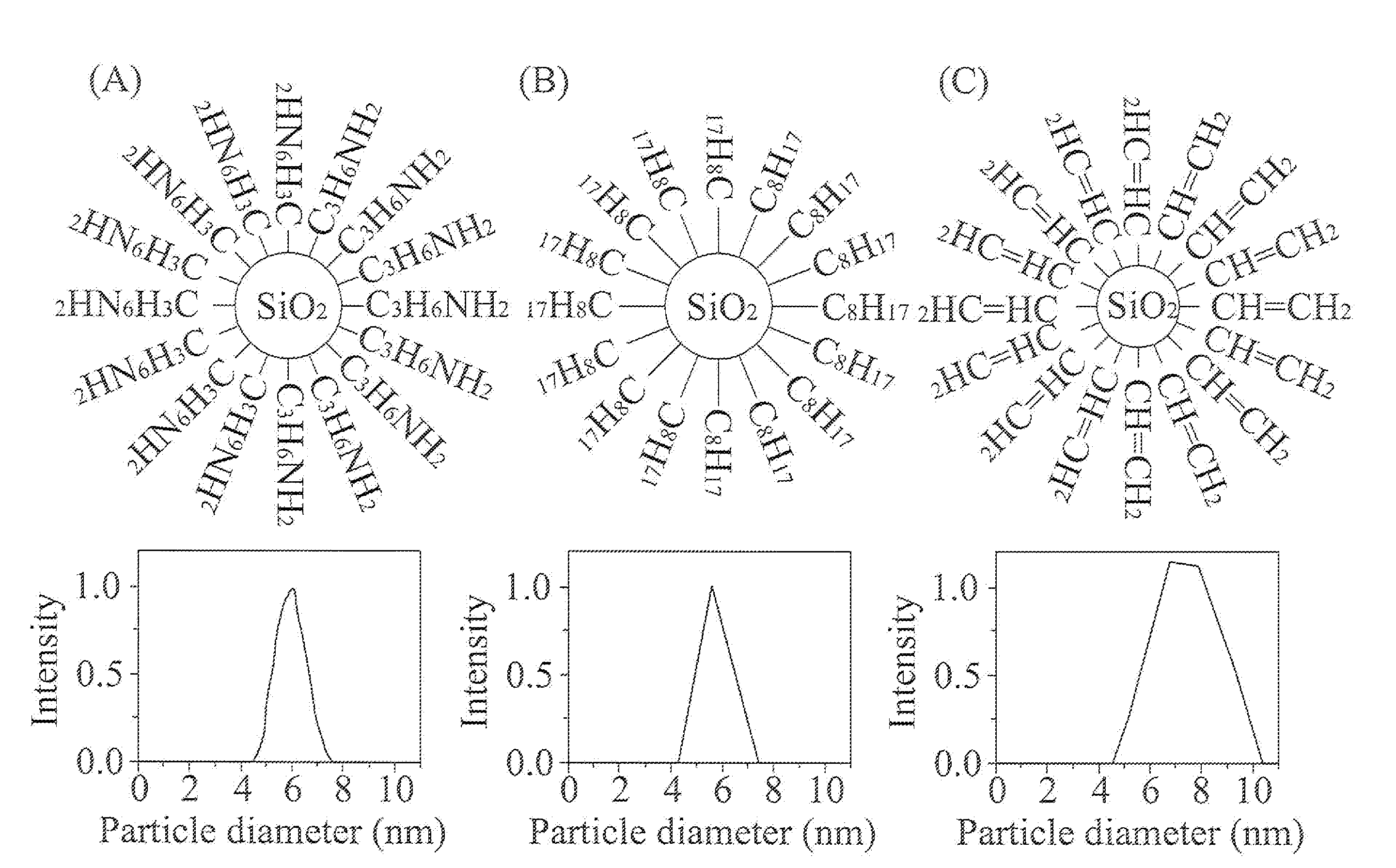
[0019]Referring to FIG. 1, there is shown a schematic illustration of the molecular structure of each type of modified nano-dots according to the present is invention. Also shown are the profiles of their particle size. In this figure, FIG. 1(A) illustrates a polymeric silicon-oxide nano-dot with 3-aminopropyltriethoxysilane on the surface. Its particle size is in the range of 4-8 nm. FIG. 1(B) illustrates a polymeric silicon-oxide nano-dot with n-octyltrimethoxysilane on the surface. Its particle size is in the range of 4-8 nm. FIG. 1(C) illustrates a polymeric silicon-oxide nano-dot with vinyltrimethoxysilane on the surface. Its particle size is in the range of 5-11 nm.

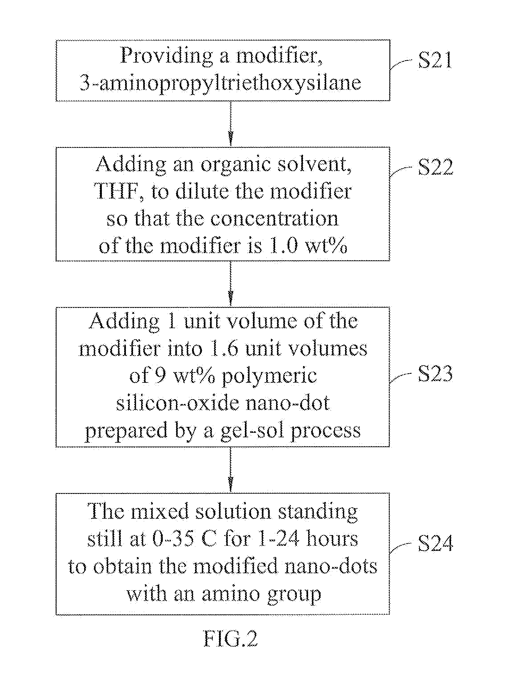
[0020]Referring to FIG. 2, there is shown a flow chart of a fabrication method of the modified nano-dot in FIG. 1(A). The steps are as follows: step S21, providing a modifier, 3-aminopropyltriethoxysilane; step S22, adding an organic solvent, tetrahydrofuran (THF), to dilute the modifier so that the weight percent c...


PUM

PropertyMeasurementUnit
particle sizeaaaaaaaaaa

Abstract

The present invention discloses a modified nano-dot and a fabrication method thereof. The modified nano-dot comprises a surface portion having a functional group and a core portion comprising a polymeric metal oxide, polymeric metalloid oxide or polymeric metal alloy oxide. The mean particle size of the modified nano-dot is 1-100 nm, preferably 1-10 nm. The modified nano-dot capable of modulating a carrier flux can be further applied to the element manufacture in the organic semiconductor industry, optoelectronics industry, and solar cell industry.

Description

CROSS REFERENCE[0001]This is a division of U.S. application Ser. No. 12 / 660,556, filed Mar. 1, 2010 for MODIFIED NANO-DOT, FABRICATION METHOD THEREOF AND COMPOSITION ELEMENT THEREOF, which claims priority to Taiwanese Patent Application No. 098107023 filed Mar. 4, 2009.BACKGROUND OF THE INVENTION[0002](a) Field of the Invention[0003]The present invention relates a modified nano-dot, a fabrication method thereof and a composition element thereof, and more particularly to a modified nano-dot for modulating a carrier flux.[0004](b) Description of the Prior Art[0005]Currently, it has been known that polymeric nano-dots (PNDs) can effectively improve the device efficiency of organic light emitting diodes and are suitable for use in high quality displays and large area illumination. In contrast to dry-processed electrically neutral quantum-dots and nano-dots, polymeric nano-dots can be synthesized with precisely controlled size and wet-processed on soft substrates, enabling the realizatio...

Claims


Application Information

Patent Timeline
Patent Type & Authority Applications(United States)
IPC IPC(8): C09K11/06B82Y30/00
CPCB82Y30/00C01P2004/64H05B33/22C09C1/3081H01L51/5012C01P2006/40H10K50/11
Inventor JOU, JWO-HUEIWANG, WEI-BENHSU, MAO-FENGCHEN, CHENG-CHUNG
Owner NATIONAL TSING HUA UNIVERSITY
Why Eureka
Try Eureka