Fabrication Method of Flexible Devices

a technology of flexible devices and fabrication methods, which is applied in the direction of semiconductor devices, electrical/magnetic/electromagnetic heating, electrical apparatus, etc., can solve the problems of difficult handling of the fabrication process, insufficient research into reliable flexible device fabrication processes for commercialization and mass production, and complicating the fabrication process. , to achieve the effect of easy separation of plastic substrates

Active Publication Date: 2012-03-15
KOREA ADVANCED INST OF SCI & TECH
View PDF3 Cites 25 Cited by
  • Summary
  • Abstract
  • Description
  • Claims
  • Application Information

AI Technical Summary

Benefits of technology

[0006]Accordingly, the present invention has been made keeping in mind the problems encountered in the related art and the present invention is intended to provide a method of fabricating a flexible device, which includes forming a plastic substrate equipped with chemical and heat resistance adapted for the processing conditions used when fabricating a device on a carrier plate, forming a device on the plastic substrate, and then easily separating the plastic substrate from the carrier plate.
[0007]Also the present invention is intended to provide a method of fabricating a flexible device in which a plastic substrate having a low coefficient of thermal expansion is used for reliable fabrication of flexible devices without using either an adhesive or a laser release technique when the plastic substrate is formed on or separated from the carrier plate.

Problems solved by technology

Despite this being such an era and there being a technical demand, however, research into reliable flexible device fabrication processes for commercialization and mass production is still insufficient.
The case of fabricating devices directly onto freestanding plastic substrates is disadvantageous because the device is directly manufactured on a plastic substrate without a carrier plate, making it difficult to handle the fabricating process due to the absence of the carrier plate and to reliably manufacture the device due to severe deformation of the plastic substrate.
In this case, however, the adhesive may be left behind, undesirably causing contamination, and also the additional separation process is inevitably performed attributed to the use of the organic solvent.
However, these methods are problematic because the amorphous silicon sacrificial layer functioning to attach the plastic substrate should be provided, undesirably complicating the fabrication process.
In particular, because a laser is used during the transfer and separation processes, the yield is undesirably reduced and the process cost is increased.

Method used


Image

  • Fabrication Method of Flexible Devices
  • Fabrication Method of Flexible Devices

Examples


example 1

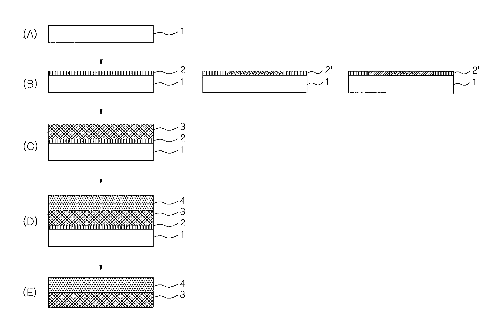
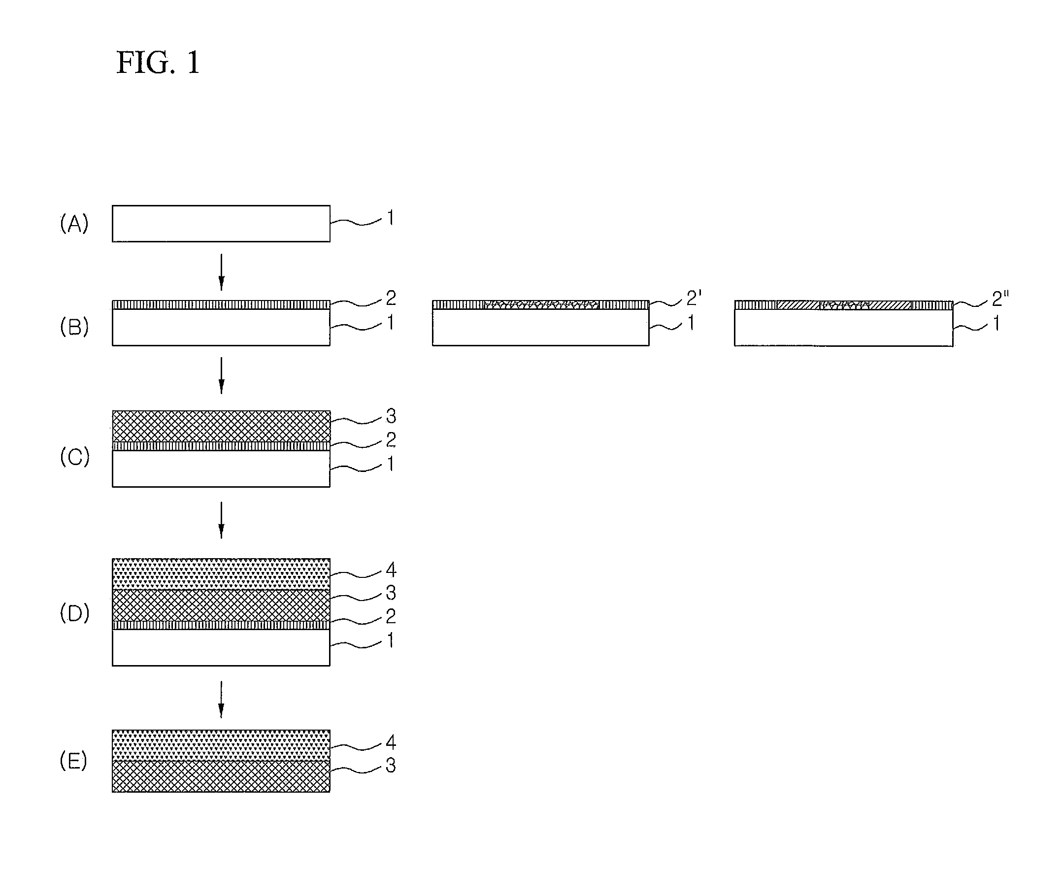
[0030]A glass plate was cut to a size of 10 cm×10 cm, and then subjected to oxygen plasma treatment. Subsequently, the center region of the glass plate except the four sides thereof having a width of 1 cm was deposited with 1H,1H,2H,2H-heptadecafluorodecyltrimethoxysilane. On the glass plate thus surface-treated, a 50 μM-thick glass fabric (E-glass, Nittobo, Japan) was disposed, and a siloxane resin (MD or HMD Hybrimer, KAIST, Korea) having methacryl groups and phenyl groups was coated thereon and thus impregnated therein. While pressure was applied thereto, 365 nm UV was irradiated for 5 min in a nitrogen atmosphere, thus forming a glass-fiber reinforced plastic substrate film on the carrier plate. On the glass-fiber reinforced plastic substrate film formed on the surface-treated glass plate, atomic layer deposition (ALD) and radio frequency (RF) sputtering were performed at 150° C., thus fabricating an oxide semiconductor thin film transistor. Thereafter, the glass-fiber reinforce...

example 2

[0031]A glass plate was cut to a size of 10 cm×10 cm, and then subjected to oxygen plasma treatment. Subsequently, the glass plate was surface-treated in such a manner that the center region of the glass plate except the four sides thereof having a width of 1 cm was coated with a siloxane resin (ED Hybrimer, KAIST, Korea) having epoxy groups and phenyl groups to form a thin film. Subsequently, two 25 μm-thick sheets of glass fabric (E-glass, Nittobo, Japan) were disposed on the surface-treated glass plate, and a siloxane resin (MD or HMD Hybrimer, KAIST, Korea) having methacryl groups and phenyl groups was coated thereon and thus impregnated therein. While pressure was applied thereto, 365 nm UV was irradiated for 5 min in a nitrogen atmosphere, thus forming a glass-fiber reinforced plastic substrate film on the carrier plate. ALD and RF sputtering were performed at 150° C. on the glass-fiber reinforced plastic substrate film formed on the surface-treated glass plate, thus fabricati...

example 3

[0032]A glass plate was cut to a size of 10 cm×10 cm, and then subjected to oxygen plasma treatment. Subsequently, the glass plate was surface-treated in such a manner that four sides of the glass plate having a width of 1 cm were coated with a polydophamine aqueous solution resin to form a thin film and the center region thereof was deposited with 1H,1H,2H,2H-heptadecafluorodecyltrimethoxysilane. On the glass plate thus surface-treated, two 25 μm-thick sheets of glass fabric (E-glass, Nittobo, Japan) were disposed, and a siloxane resin (ED Hybrimer, KAIST, Korea) having epoxy groups and phenyl groups was coated thereon and thus impregnated therein. 365 nm UV was then irradiated for 5 min, thus forming a glass-fiber reinforced plastic substrate film on the carrier plate. ALD and RF sputtering were performed at 150° C. on the glass-fiber reinforced plastic substrate film formed on the surface-treated glass plate, thus fabricating an oxide semiconductor thin film transistor. Thereafte...


PUM

PropertyMeasurementUnit
sizeaaaaaaaaaa
widthaaaaaaaaaa
transparentaaaaaaaaaa

Abstract

Disclosed is a method of fabricating a flexible device, which includes surface-treating one or both sides of a carrier plate so that regions with different surface-treatments are formed on the same side of the carrier plate, forming a glass-filler reinforced plastic substrate film on the surface-treated carrier plate, forming thin film patterns on the glass-filler reinforced plastic substrate film, and separating the glass-filler reinforced plastic substrate film having the thin film patterns formed thereon from the carrier plate, and in which the surface-treating of the carrier plate enables the glass-filler reinforced plastic substrate film to be easily separated from the carrier plate without an additional process such as using a solvent or a laser release technique.

Description

BACKGROUND OF THE INVENTION[0001]1. Technical Field[0002]The present invention relates to a method of fabricating a flexible device, and more particularly to a method of fabricating a flexible device, which enables an electronic, photoelectronic or energy device including a display to be reliably manufactured on a plastic substrate and also which enables a plastic substrate formed on a carrier plate to be easily separated from the carrier plate without an additional separation process thus facilitating the fabrication of the device.[0003]2. Description of the Related Art[0004]Recently, thorough research into flexible devices to develop electronic, photoelectronic, and energy devices including conventional flat panel displays, having environment-friendly properties, low power consumption, small sizes, lightweight, and flexibility, is ongoing. In order to enable flexible devices, a flexible substrate should be used as the most fundamental starting component. Typically useful candidate...

Claims


Application Information

Patent Timeline
Patent Type & Authority Applications(United States)
IPC IPC(8): B29C59/16B29C33/42
CPCH01L21/6835H01L2221/6835H01L2221/68318
Inventor BAE, BYEONG-SOOJIN, JUNGHO
Owner KOREA ADVANCED INST OF SCI & TECH
Why Eureka
Try Eureka