Conductive path in switching material in a resistive random access memory device and control

a random access memory and switching material technology, applied in the direction of bulk negative resistance effect devices, basic electric elements, electric devices, etc., can solve the problems of increasing power dissipation, sub-threshold slope non-scaling, and reducing device performance, so as to achieve low forming voltage, broader range of applicability, and low leakage current

Active Publication Date: 2012-03-29
INNOSTAR SEMICON SHANGHAI CO LTD
View PDF7 Cites 86 Cited by
  • Summary
  • Abstract
  • Description
  • Claims
  • Application Information

AI Technical Summary

Benefits of technology

[0007]The present invention is related to switching devices. More particularly, the present invention is provides a resistive switching device characterized by a low forming voltage and a low leakage current. Embodiments of the present invention have been applied to fabrication and operation of a resistive random access memory (RRAM) device. But it should be recognized that the present invention can have a much broader range of applicability.
[0008]In a specific embodiment, a resistive switching device is provided. The resistive switching device includes a first electrode, a switching material, and a second electrode. In a specific embodiment, the resistive switching device includes a thickness of dielectric material disposed between the second electrode and the switching material. The thickness of dielectric material is configured to electrically breakdown in a region and cause formation of an open region in a portion of...

Problems solved by technology

However, as field effect transistors (FET) approach sizes less than 100 nm, problems such as short channel effect can degrade device performance.
Moreover, such sub 100 nm device size can lead to sub-threshold slope non-scaling and also increases power dissipation.
These devices often require new materials and device structures to couple with silicon-based devices to form a memory cell, ...

Method used


Image

  • Conductive path in switching material in a resistive random access memory device and control
  • Conductive path in switching material in a resistive random access memory device and control
  • Conductive path in switching material in a resistive random access memory device and control

Examples


Embodiment Construction

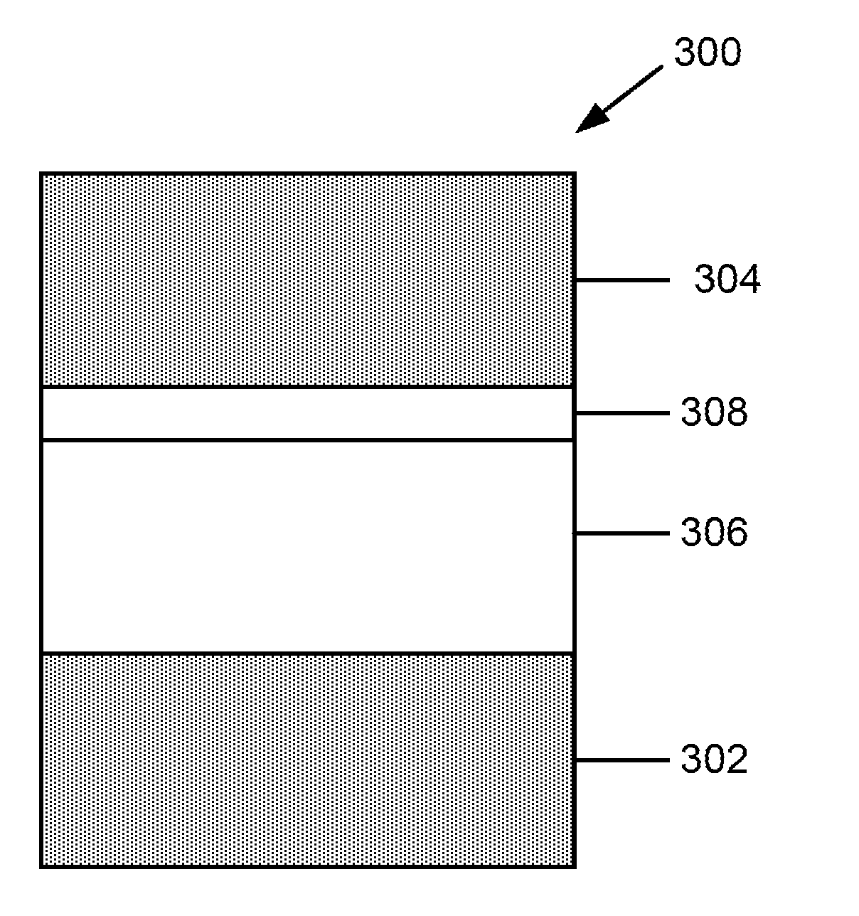
[0021]The present invention is related to switching devices. More particularly, the present invention provides a resistive switching device characterized by a well controlled electroforming process and a low leakage current. Embodiments of the present invention have been applied to fabrication and operation of a resistive random access memory device. But it should be recognized that the present invention can have a much broader range of applicability.

[0022]Due to the explosive growth in consumer devices, there is an ever increasing demand for memory device density. Data storage of current non-volatile memory devices are based on charges stored in a floating gate or a dielectric layer. Scaling of these devices is limited as these devices usually require a transistor device coupled to a memory cell. Further down scale of transistors may not be possible due to short channel effects and others.

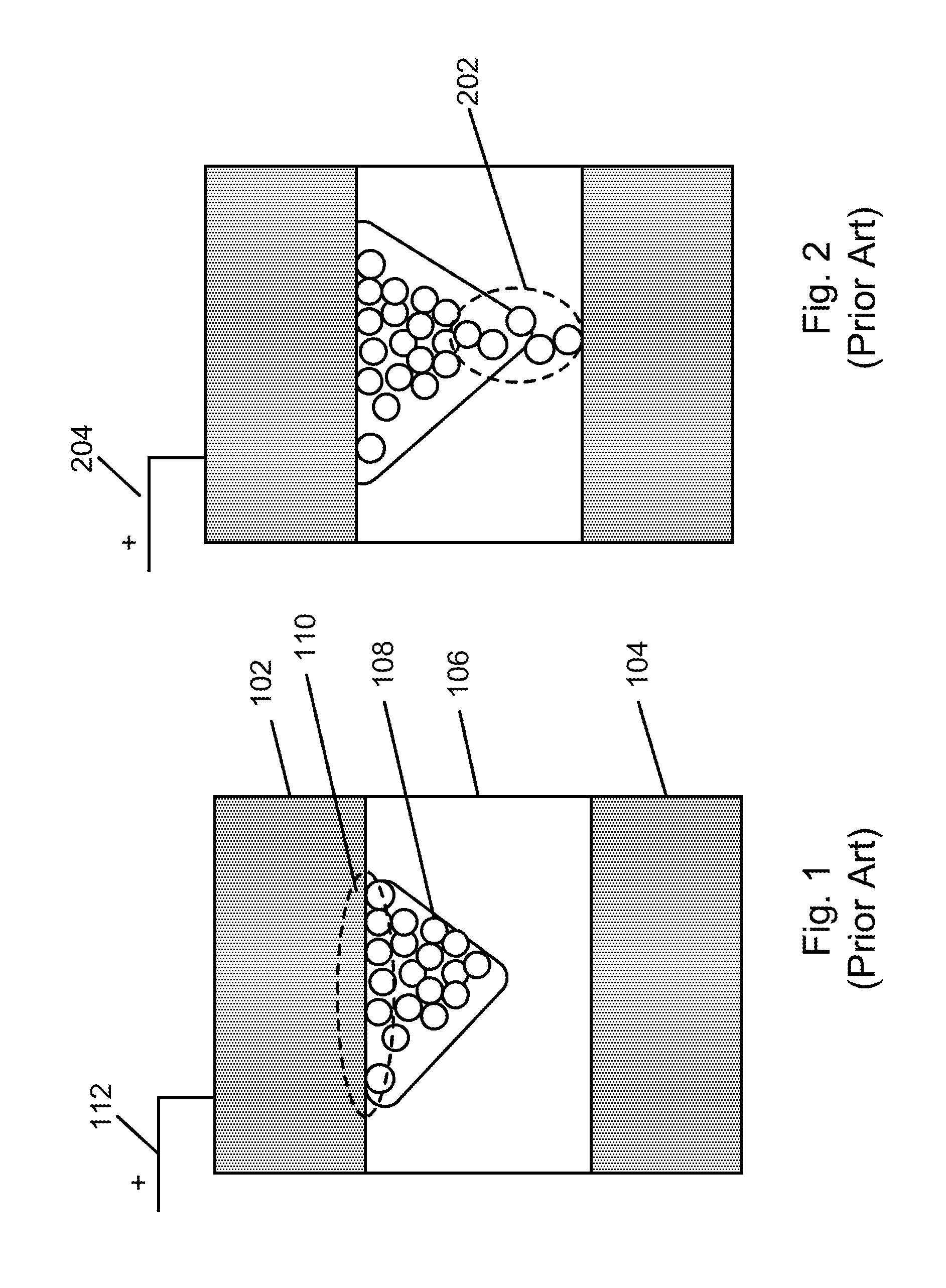
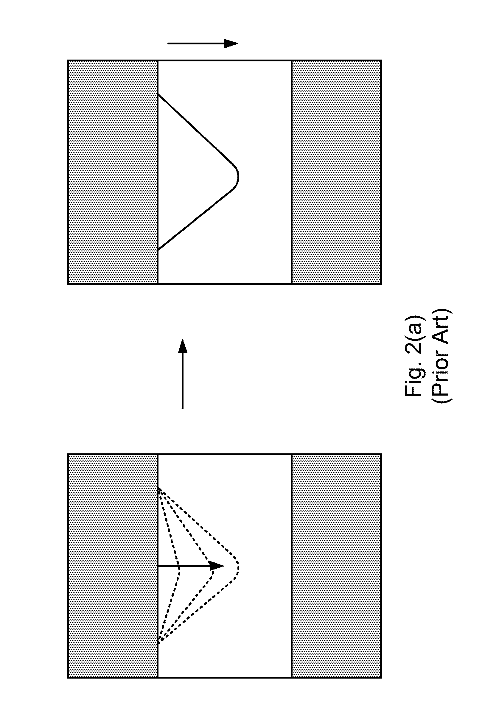
[0023]Resistive switching in an amorphous silicon based resistive random access memory (RRAM) ...


PUM


Abstract

A non-volatile memory device structure. The device structure includes a first electrode, a second electrode, a resistive switching material comprising an amorphous silicon material overlying the first electrode, and a thickness of dielectric material having a thickness ranging from 5 nm to 10 nm disposed between the second electrode and the resistive switching layer. The thickness of dielectric material is configured to electrically breakdown in a region upon application of an electroforming voltage to the second electrode. The electrical breakdown allows for a metal region having a dimension of less than about 10 nm by 10 nm to form in a portion of the resistive switching material.

Description

CROSS REFERENCE TO RELATED APPLICATIONS[0001]Not ApplicableSTATEMENT RELATED TO GOVERNMENT OR FEDERAL SPONSORED RESEARCH[0002]Not ApplicableBACKGROUND[0003]The present invention is related to switching devices. More particularly, the present invention is provides a resistive switching device characterized by a reduced forming voltage and a low leakage current. Embodiments of the present invention have been applied to fabrication and operation of a resistive random access memory device. But it should be recognized that the present invention can have a much broader range of applicability.[0004]The success of semiconductor devices has been mainly driven by an intensive transistor down-scaling process. However, as field effect transistors (FET) approach sizes less than 100 nm, problems such as short channel effect can degrade device performance. Moreover, such sub 100 nm device size can lead to sub-threshold slope non-scaling and also increases power dissipation. It is generally believe...

Claims


Application Information

Patent Timeline
IPC IPC(8): H01L45/00H01L21/02
CPCH01L45/085H01L45/148H01L45/1233H01L45/12H10N70/245H10N70/801H10N70/884H10N70/826
Inventor JO, SUNG HYUN
Owner INNOSTAR SEMICON SHANGHAI CO LTD
Why Eureka
Try Eureka