Optical device, a method of manufacturing optical device, and exposure apparatus

a manufacturing method and optical technology, applied in the field of optical devices, can solve the problems of difficult to maintain uniform accuracy over a wide surface area, difficult for this optical modulator to perform modulation at a high speed, etc., to achieve the effect of reducing the driving voltage, reducing the thickness of ferroelectric crystals, and reducing the thickness of optical components

Active Publication Date: 2012-04-05
DAINIPPON SCREEN MTG CO LTD
View PDF2 Cites 8 Cited by
  • Summary
  • Abstract
  • Description
  • Claims
  • Application Information

AI Technical Summary

Benefits of technology

[0006]By the way, while the optical modulator according to the Document 1 is capable of modulating light due to the electro-optical effect, it is difficult to for this optical modulator to perform modulation at a high speed since the thickness of the ferroelectric crystals is approximately 300 μm, the domain-inverted period is as rough as 40 μm and the required driving voltage must be as high as 25 V or more. Hence, it is necessary to decrease the driving voltage in order to realize even faster modulation. One of the approaches to achieve this is to reduce the thickness of the ferroelectric crystals (which is k

Problems solved by technology

By the way, while the optical modulator according to the Document 1 is capable of modulating light due to the electro-optical effect, it is difficult to for this optical modulator to perform modulation at a high speed since the thickness of the ferroelectric crystals is appro

Method used


Image

  • Optical device, a method of manufacturing optical device, and exposure apparatus
  • Optical device, a method of manufacturing optical device, and exposure apparatus
  • Optical device, a method of manufacturing optical device, and exposure apparatus

Examples


first embodiment

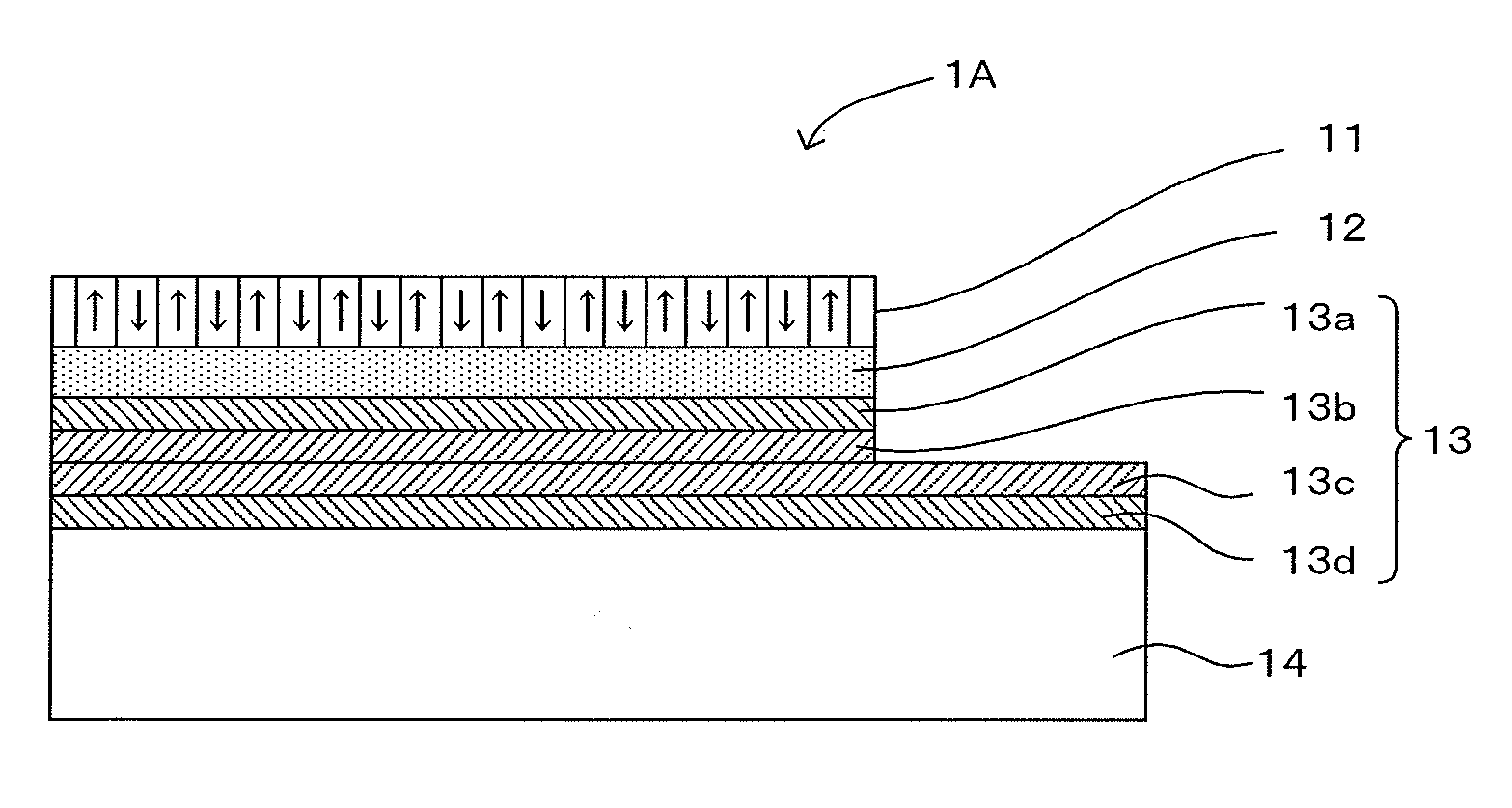
[0033]FIG. 1 is a cross sectional view which shows a first embodiment of an optical device according the invention. The optical device 1A comprises a ferroelectric substrate 11 formed by periodically domain inverted (periodically poled) ferroelectric crystals, and a support plate 14 supports the ferroelectric substrate 11 via an insulation layer 12 of SiO2 or the like and a junction 13 which has a quadruple-layer structure. In this embodiment, processing described later is performed on a single crystal substrate of lithium niobate (MgO:lithium niobate) added with magnesium oxide (MgO) or stoichiometric lithium tantalite (MgO:stoichiometric lithium tantalite) added with magnesium oxide (MgO), whereby the periodically domain inverted ferroelectric substrate 11 is formed as a thin film. Lithium niobate added with magnesium oxide (MgO) will be hereinafter referred to as “MgO:LN” and stoichiometric lithium tantalite added with magnesium oxide will be hereinafter referred to as “MgO:SLT.”...

second embodiment

[0056]FIGS. 5A and 5B are cross sectional views which show a second embodiment of the optical device according to the invention. FIG. 5A shows the overall structure, and FIG. 5B is an enlarged schematic diagram of the section enclosed by the dotted line in FIG. 5A. FIGS. 6A through 6C are schematic diagrams of the manufacturing method of the optical device shown in FIGS. 5A and 5B, but show only characteristic steps of the manufacturing method according to the second embodiment. A major difference of the second embodiment from the first embodiment is the structure of the junction 13, and the other structures remain the same as those according to the first embodiment. Therefore, redundant descriptions will be omitted on the same structures which will instead be denoted at the same reference symbols.

[0057]In the second embodiment, the chromium film 13a and the gold film 13b forming the first metal layer are patterned in the arrangement pattern of the concave sections 15a formed in the...

third embodiment

[0066]FIGS. 7A through 7D are cross sectional views which show a third embodiment of the optical device according the invention. The optical device 1C according to the third embodiment is integration of the ferroelectric substrate 11 formed by ferroelectric crystals having periodically poled structure and the support plate 14, which is thicker than the ferroelectric substrate 11, via the quadruple-layer junction 13 as shown in FIG. 7D, and is manufactured in the following manner.

[0067]The third embodiment requires preparing the ferroelectric substrate 11 formed by ferroelectric crystals having periodically poled structure and the support plate 14. As in the first and the second embodiments, the support plate 14 has the same composition as that of the ferroelectric substrate 11 and is formed by ferroelectric crystals having the same absolute value of the crystal orientation as that of the ferroelectric substrate 11 according to the third embodiment. Through sputtering or deposition, ...


PUM


Abstract

The ferroelectric substrate 11 of ferroelectric crystals, while being supported by the support plate 14 which is thicker than the ferroelectric substrate 11, is integrated with the support plate 14 by letting the junction 13 mediate between one major surface S1A of the ferroelectric substrate 11 and one major surface S1B of the support plate 14, and therefore, it is possible through the flat surface polishing to perform thinning of the ferroelectric substrate 11, namely, the ferroelectric crystals, and as a result, it is possible to obtain the thin periodically poled structure. By the voltage application method, the domain inverted region is formed in the ferroelectric substrate 11 which is made thin.

Description

CROSS REFERENCE TO RELATED APPLICATION[0001]The disclosure of Japanese Patent Application No. 2010-221699 filed Sep. 30, 2010 including specification, drawings and claims is incorporated herein by reference in its entirety.BACKGROUND OF THE INVENTION[0002]1. Field of the Invention[0003]The present invention relates to an optical device having a periodically poled structure (hereinafter referred to simply as the “optical device”), a method of manufacturing the optical device and an exposure apparatus which uses the optical device.[0004]2. Description of the Related Art[0005]Ferroelectric crystals of lithium niobate (LiNbO3), lithium tantalite (LiTaO3) and the like have been under consideration as liquid crystals to be applied to optical devices for controlling light modulation, wavelength conversion, etc. The Document 1 (H. Gnewuch et al “Nanosecond Response of Bragg Deflectors in Periodically Poled LiNbO3”, IEEE PHOTONICS TECHNOLOGY LETTERS, VOL. 10, NO. 12, DECEMBER 1998) for insta...

Claims


Application Information

Patent Timeline
IPC IPC(8): G02F1/05
CPCG02F1/3558G02F1/2955G02F1/292G02F1/3775
Inventor OKAZAKI, MASAHIDESUHARA, TOSHIAKI
Owner DAINIPPON SCREEN MTG CO LTD
Why Eureka
Try Eureka