Charged particle radiation device

a radiation device and charged particle technology, applied in the field can solve the problems of deterioration in resolution of charged particle radiation devices, and deterioration in picture quality, so as to prevent the occurrence of loop of force and current loop, high resolution, and the effect of reducing the natural vibration of the ion pump

Active Publication Date: 2012-04-19
HITACHI HIGH-TECH CORP
View PDF13 Cites 10 Cited by
  • Summary
  • Abstract
  • Description
  • Claims
  • Application Information

AI Technical Summary

Benefits of technology

[0021]In the charged particle radiation device according to the invention, it is possible to attenuate the natural vibration of the ion pump after movement of the stage in a short time, and to prevent the occurrence of the loop of force and the loop of current. As a result, an observation image high in resolution can be acquired at a high speed.

Problems solved by technology

For this reason, vibration of the electron optical lens tube will invite deterioration in picture quality of the observation image, and further, this will create a factor that will induce deterioration in resolution of the charged particle radiation device.
The electron optical lens tube is vibrated due to vibration of an ion pump that can be regarded as an added mass of the electron optical lens tube after stoppage of movement of a stage on which a sample is placed, thereby raising a possibility of causing deterioration in the picture quality.
Accordingly, there exists a problem that the ion pump becomes complex in structure and baking becomes difficult to apply because a viscoelastic damper that will be cured by heating is disposed inside the ion pump.
However, there exists a problem that an advantageous effect of from the device itself, such as vibration occurring due to movement of a stage, cannot be expected.

Method used


Image

  • Charged particle radiation device
  • Charged particle radiation device
  • Charged particle radiation device

Examples


first embodiment

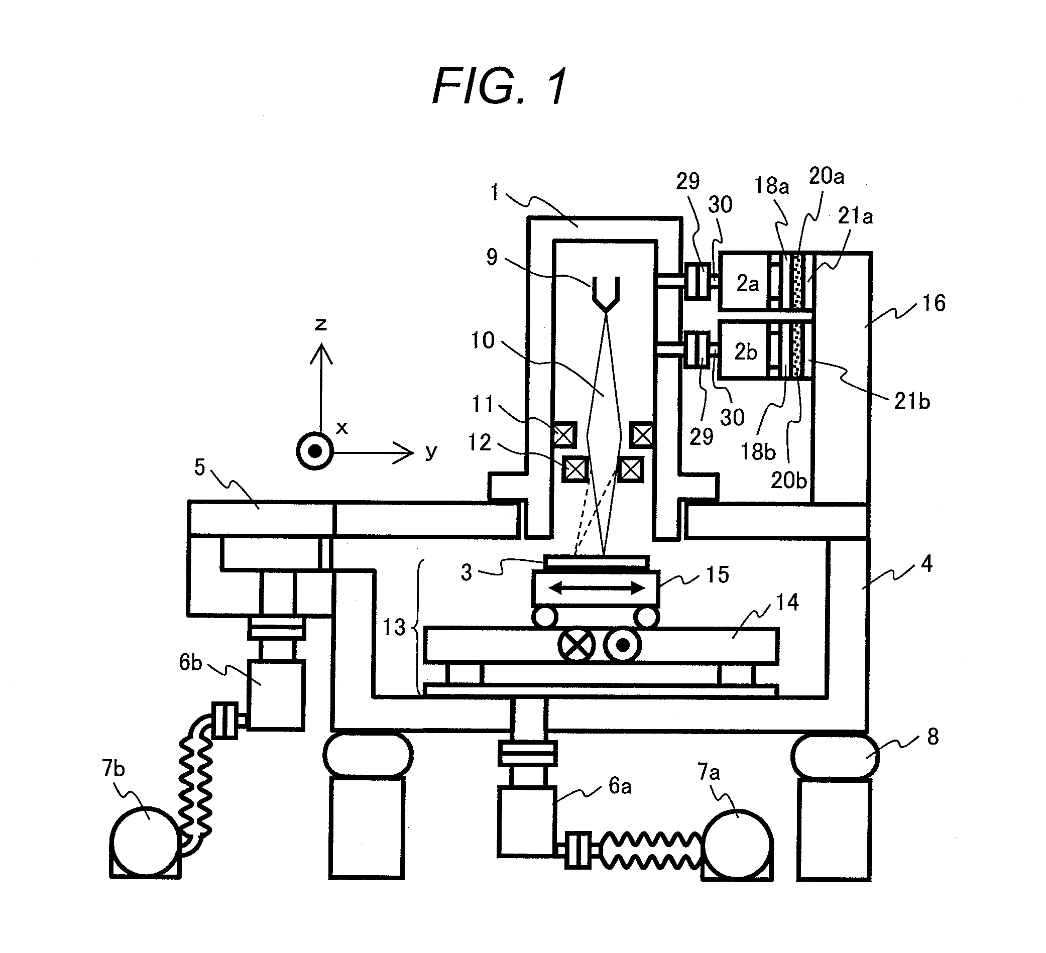
[0052]A charged particle radiation device according to the first embodiment of the invention is described hereinafter by citing a semiconductor inspection device as an example. FIG. 1 is a schematic view showing a semiconductor inspection device according to the first embodiment of the invention.

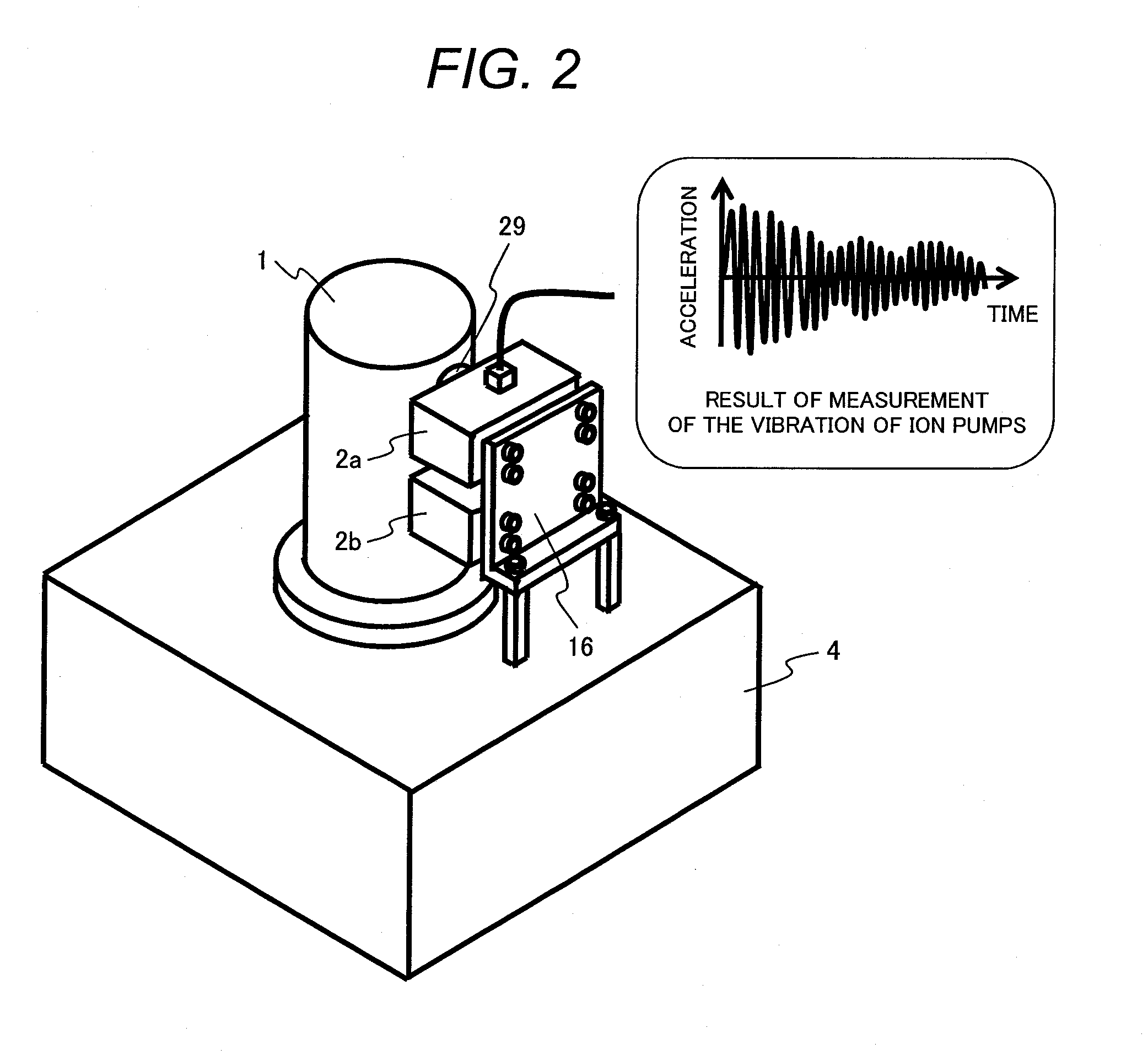
[0053]An electron optical lens tube 1 of the semiconductor inspection device is evacuated by two units of ion pumps 2a and 2b, and an ultra-high vacuum state is maintained inside the electron optical lens tube 1. A stage 13 with a sample 3 mounted thereon moves inside a sample chamber 4. The sample chamber 4 is evacuated by a turbo-molecular pump 6a and a roughing vacuum pump 7a. A load lock chamber 5 for delivering the sample 3 to the outside device is also evacuated by the turbo-molecular pump 6b and the roughing vacuum pump 7b.

[0054]A damping mount 8 attenuates the vibration propagating from the floor to the semiconductor inspection device.

[0055]An electron beam 10 emitted from an electr...

second embodiment

[0064]A charged particle radiation device according to the second embodiment of the invention is described hereinafter by citing a scanning electron microscope as an example. FIG. 9 is a schematic view showing a scanning electron microscope according to the second embodiment of the invention.

[0065]While the semiconductor inspection device according to the first embodiment, shown in FIG. 1, is a device for use in observation of a sample large in diameter, the scanning electron microscope shown in FIG. 9 is a device for use in observation of a sample small in size. Accordingly, a sample chamber 24 is small and is mounted on a load plate 23. The load plate 23 is a plate-shaped member for supporting the sample chamber 24 and installed over a damping mount (not shown) for blocking vibration from the floor.

[0066]A method for attaching ion pumps 2a and 2b to an electron optical lens tube 1, and methods for attaching metal plates 18a and 18b, viscoelastic sheets 20a and 20b, and metal plate...

third embodiment

[0069]A charged particle radiation device according to the third embodiment of the invention is described hereinafter by citing a semiconductor inspection device as an example, as is the case with the first embodiment. FIG. 10 is a schematic view showing a semiconductor inspection device according to the third embodiment of the invention.

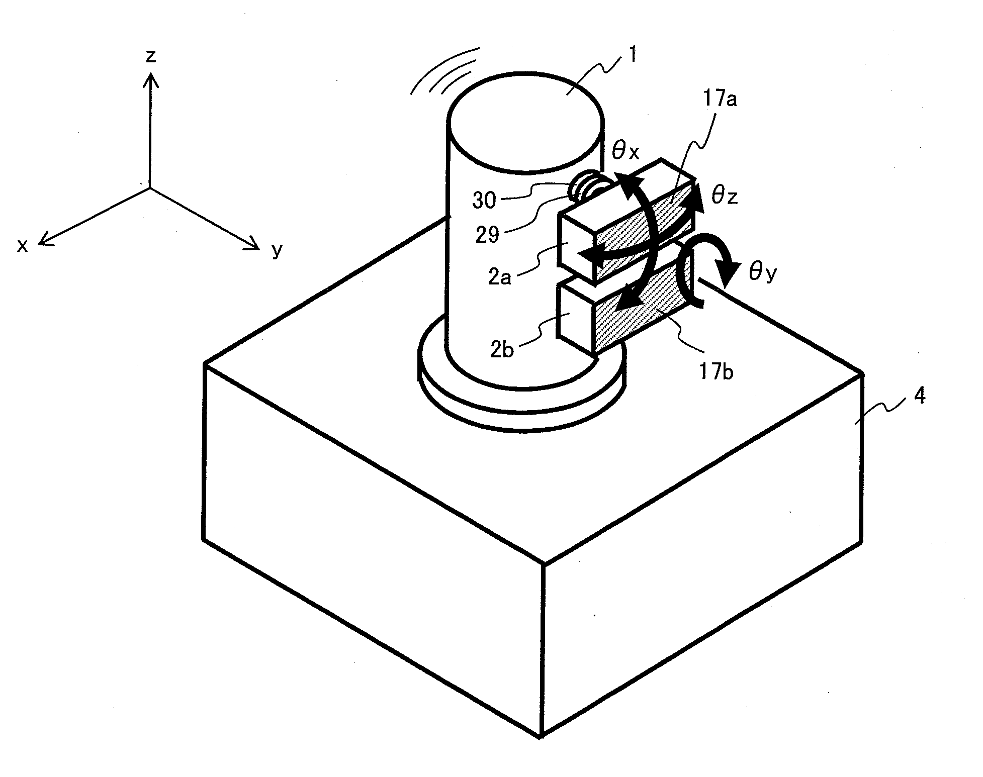
[0070]Even in the configuration of the semiconductor inspection device according to the first embodiment, the angles of rotation around the x-axis, y-axis, and z-axis can be adjusted, respectively. The fitting faces 17a and 17b of the ion pumps 2a and 2b, respectively, are ideally to be parallel to the x-z plane. However, since the ion pumps 2a and 2b are attached to the electron optical lens tube 1 by welding as previously described, the fitting faces 17a and 17b are not exactly aligned with each other in respect of position and orientation, and the fitting faces 17a and 17b are occasionally oriented in differing directions from each other. That is...


PUM


Abstract

Disclosed is a high resolution and high throughput charged particle radiation device that attenuates the natural vibration of an ion pump in a short time, excited by a reaction force at the time of driving the stage, and prevents occurrence of a loop of force and a loop of current. The charged particle radiation device includes a sample chamber (4) for disposing a sample (3) therein, a charged particle radiation optical lens tube (1) for irradiating the sample (3) with charged particle radiation (10), ion pumps (2a, 2b) for evacuating the charged particle radiation optical lens tube (1), a frame (16) fixedly attached to the sample chamber (4), the frame (16) facing one end of each of the ion pumps (2a, 2b), and vibration absorbers provided between the frame (16) and the one end of each of the ion pumps (2a, 2b), each of the vibration absorbers including a layered structure which includes a viscoelastic sheet (20a, 20b) sandwiched between metal plates (18a, 18b, 21a, 21b).

Description

TECHNICAL FIELD[0001]The present invention relates to a charged particle radiation device, and in particular, to a charged particle radiation device provided with an ion pump.BACKGROUND ART[0002]In a charged particle radiation device, such as a scanning electron microscope, a transmission electron microscope, and a semiconductor inspection device, a sample is irradiated with charged particle radiation (an electron beam) generated in an ultra-high vacuum environment inside an electron optical lens tube, and a secondary electron, a reflection electron, or a transmission electron from the sample is detected, thereby acquiring an observation image of the sample. If the electron optical lens tube is vibrated, this will cause a change in a position of the electron beam irradiation to the sample, so that strain occurs to the observation image, and the edge of a pattern is seen as vibrating, or in the case of adding up the plurality of observation images, the edge of an image after addition...

Claims


Application Information

Patent Timeline
Patent Type & Authority Applications(United States)
IPC IPC(8): H01J37/20
CPCF16F9/306H01J2237/0216H01J37/16
Inventor TSUJI, HIROSHIISHIGURO, KOUJITACHIBANA, ICHIROSUZUKI, NAOMASAONUKI, KATSUNORI
Owner HITACHI HIGH-TECH CORP
Why Eureka
Try Eureka