
Eureka
For R&D, Eureka makes reading and utilizing patents & technical documents easy.
Eureka AIR
Designed for self-driven R&D workflows. Generate viable solutions, solve complex R&D challenges, empower your innovation with AI.

Eureka Materials
Designed for material experts only. Revolutionize your material R&D, from search, analyze, to developing new materials.

TechResearch
Generate reliable direction feasibility study reports for your R&D in just a few steps.

TechSeek
Discover and master advanced knowledge NOW. Basics, ideas, possibilities, all at once.

TechMind
As an expert in R&D Theories, TechMind can generates customized viable solutions instantly.

TechRisk
Analyze your overall solution with one click, know your potential R&D risks in advance.

TechMonitor
Get weekly tech updates, stay abreast of the latest tech innovations and key insights.
Method for manufacturing semiconductor device
- Summary
- Abstract
- Description
- Claims
- Application Information
AI Technical Summary
Benefits of technology
Problems solved by technology
Method used
Image

Examples
embodiment 1
[0045]In this embodiment, a method for manufacturing a semiconductor device that is one embodiment of the present invention will be described with reference to drawings.
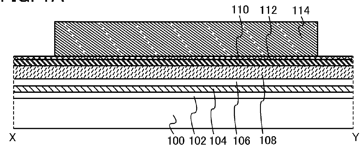
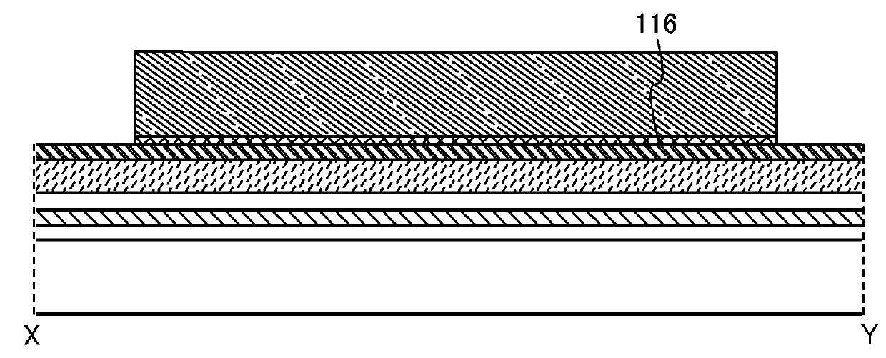
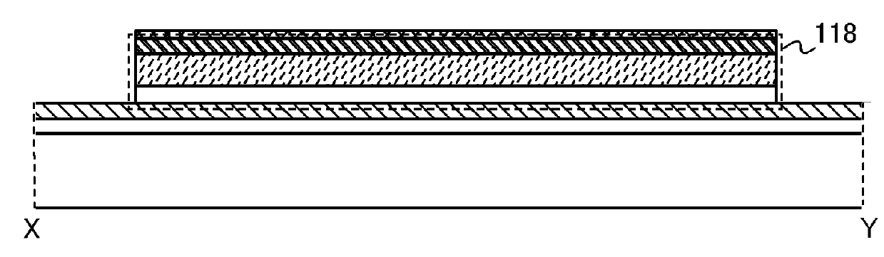
[0046]A method for manufacturing a semiconductor device of one embodiment of the present invention, which is described in this embodiment, includes the steps of: stacking a first conductive film, a first insulating film, a semiconductor film, a second conductive film, and a mask film in this order; forming a first resist mask over the mask film; forming a first mask layer by performing dry etching or wet etching on the mask film with the use of the first resist mask; removing the first resist mask using a resist stripper; forming a thin film stack body by performing dry etching on the first insulating film, the semiconductor film, and the second conductive film with the use of the first mask layer, so that a surface of the first conductive film is at least exposed; forming a second insulating film so as to cover the ...
embodiment 2
[0115]Electronic paper can be given as a semiconductor device which is one embodiment of the present invention. Electronic paper can be used for electronic appliances of a variety of fields as long as they can display data. For example, electronic paper can be applied to an electronic book reader (e-book reader), a poster, a digital signage, a public information display (PID), an advertisement in a vehicle such as a train, displays of various cards such as a credit card, and the like. An example of the electronic appliances is illustrated in FIG. 15.
[0116]FIG. 15 illustrates an example of an e-book reader. For example, an e-book reader 200 includes two housings, a housing 201 and a housing 203. The housing 201 and the housing 203 are combined with a hinge 211 so that the e-book reader 200 can be opened and closed with the hinge 211 as an axis. With such a structure, the e-book reader 200 can be handled like a paper book.
[0117]A display portion 205 and a photoelectric conversion devi...
embodiment 3
[0121]As a semiconductor device which is one embodiment of the present invention, a variety of electronic appliances (including an amusement machine) can be given in addition to electronic paper. Examples of electronic appliances are a television set (also referred to as a television or a television receiver), a monitor of a computer or the like, a camera such as a digital camera or a digital video camera, a digital photo frame, a mobile phone (also referred to as a cellular phone or a mobile phone device), a portable game console, a portable information terminal, an audio reproducing device, a large-sized game machine such as a pachinko machine, and the like.
[0122]FIG. 16A illustrates an example of a television set. A display portion 303 is incorporated in a housing 301 of a television set 300. Images can be displayed on the display portion 303. Here, the housing 301 is supported by a stand 305.
[0123]The television set 300 can be operated by an operation switch of the housing 301 o...
PUM
 Abstract
Description
Claims
Application Information
 - R&D Engineer
- R&D Manager
- IP Professional
- Industry Leading Data Capabilities
- Powerful AI technology
- Patent DNA Extraction
Browse by: Latest US Patents, China's latest patents, Technical Efficacy Thesaurus, Application Domain, Technology Topic, Popular Technical Reports.
© 2024 PatSnap. All rights reserved.Legal|Privacy policy|Modern Slavery Act Transparency Statement|Sitemap|About US| Contact US: help@patsnap.com