Thin film transistor

a thin film transistor and transistor technology, applied in the direction of transistors, semiconductor devices, electrical apparatus, etc., can solve the problems of unstable electrical specification of oxide semiconductor tft fabricated with the process aforementioned, process complicating the fabrication of conventional oxide semiconductor tft, etc., to facilitate the mass production of tft, stable electrical specification, fabrication illustrated

Active Publication Date: 2012-04-26
AU OPTRONICS CORP
View PDF3 Cites 4 Cited by
  • Summary
  • Abstract
  • Description
  • Claims
  • Application Information

AI Technical Summary

Benefits of technology

[0009]The invention is directed to a method of fabricating a TFT which facilitates the mass production of the TFT.
[0022]The TFT of the invention has stable electrical specification and the fabrication illustrated in the invention is simple and facilitates the mass production of the TFT.

Problems solved by technology

However, the oxide semiconductor TFT fabricated with the process aforementioned has unstable electrical specification (the relationship between drain current and gate voltage).
Nevertheless, this process complicates the fabrication of the conventional oxide semiconductor TFT.

Method used


Image

  • Thin film transistor
  • Thin film transistor
  • Thin film transistor

Examples


first embodiment

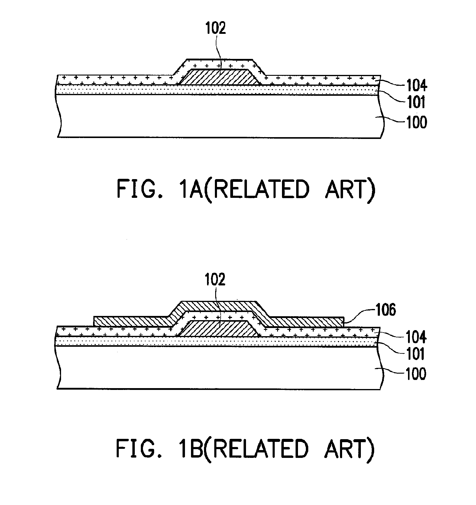
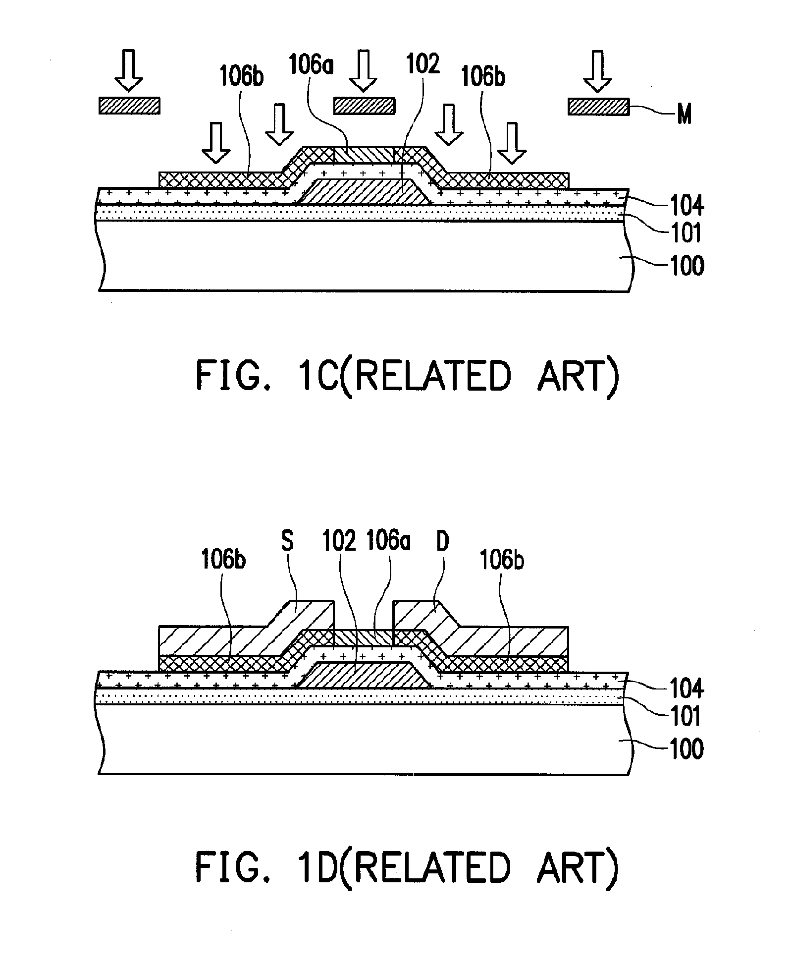
[0034]FIGS. 2A to 2E are schematic cross-sectional diagrams showing a flow chart of fabricating a TFT according to the present embodiment. Referring to FIG. 2A, a gate 202 is formed on a substrate 200. Next, a gate insulation layer 204 is formed entirely on the substrate 200 to cover the gate 202. In the present embodiment, the substrate 200 is fabricated using, for example, glass, quartz, organic polymer, non-transparent / reflective material (i.e. conductive material, wafer, ceramics and the like), or other suitable material.

[0035]In the present embodiment, a material of the gate 202 is generally a metal material. However, the invention is not limited thereto. In another embodiment, the gate 202 can also be fabricated with other conductive material such as an alloy, a nitride of a metal material, an oxide of a metal material, an oxynitride of a metal material, or a stacked layer of a metal material and other conductive material. The gate insulation layer 204 in the present embodimen...

second embodiment

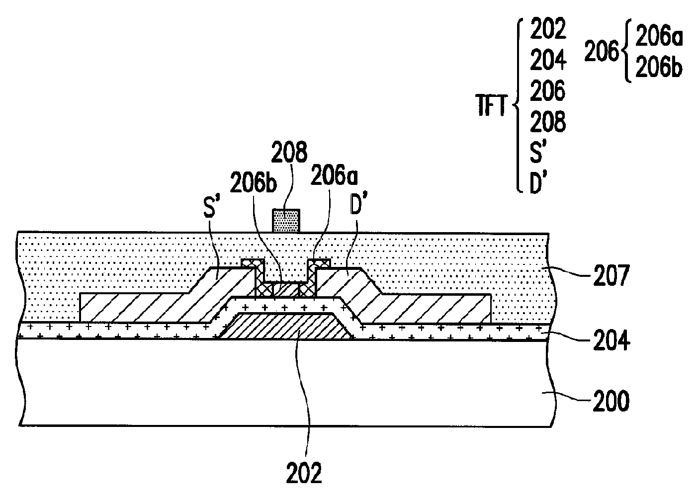
[0048]FIGS. 3A to 3E are schematic cross-sectional diagrams showing a flow chart of fabricating a TFT according to the present embodiment. Materials adopted in the composition of the TFT in the present embodiment are the same as those described in the first embodiment, and the details are omitted hereinafter.

[0049]Referring to FIG. 3A, a gate 202 is formed on a substrate 200. Next, a gate insulation layer 204 is formed entirely on the substrate 200 to cover the gate 202.

[0050]Referring to FIG. 3B, a source S′ and a drain D′ electrically insulated from each other are formed on a partial region of the gate insulation layer 204.

[0051]Referring to FIG. 3C, an oxide semiconductor layer 206 is formed on the gate insulation layer 204, the source S′ and the drain D′. In other words, the oxide semiconductor layer 206 in the present embodiment covers a portion of the gate insulation layer 204, a portion of the source S′, and a portion of the drain D′ above the gate 202.

[0052]Referring to FIG....


PUM


Abstract

A TFT including a gate, a gate insulation layer, an oxide semiconductor layer, a translucent layer, a source, and a drain. The gate insulation layer covers the gate. The oxide semiconductor layer is disposed on the gate insulation layer and located above the gate. The oxide semiconductor layer includes an oxide channel layer and two ohmic contact layers. The ohmic contact layers are respectively located beside the oxide channel layer and connected with the oxide channel layer. The translucent layer is located above the oxide channel layer. The source and the drain are disposed on the gate insulation layer and the ohmic contact layers. The source and the drain are electrically insulated from each other.

Description

CROSS-REFERENCE TO RELATED APPLICATION[0001]This is a divisional application of and claims the priority benefit of U.S. application Ser. No. 13 / 041,439, filed on Mar. 7, 2011, which claims the priority benefit of Taiwan application serial no. 99136504, filed Oct. 26, 2010. The entirety of each of the above-mentioned patent applications is hereby incorporated by reference herein and made a part of this specification.BACKGROUND OF THE INVENTION[0002]1. Field of the Invention[0003]The invention relates to a thin film transistor and a method of fabricating the same. More particularly, the invention relates to a thin film transistor having an oxide channel layer and a method of fabricating the same.[0004]2. Description of Related Art[0005]Due to increasing concerns for the environment, flat display panels with superior characteristics such as low consumption power, high space utilization efficiency, free of radiation, high image quality and so on have become the main stream in the market...

Claims


Application Information

Patent Timeline
Patent Type & Authority Applications(United States)
IPC IPC(8): H01L29/786
CPCH01L29/7869
Inventor LIN, WU-HSIUNGSUN, MING-WEI
Owner AU OPTRONICS CORP
Why Eureka
Try Eureka