Semiconductor device

a semiconductor and semiconductor technology, applied in the direction of semiconductor devices, basic electric elements, electrical apparatus, etc., can solve the problems of low robustness against surface charge, low breakdown voltage, and difficulty in realizing high breakdown voltage, and achieve high mass productivity, high breakdown voltage, and high robustness against induced surface charge

Active Publication Date: 2012-04-26
FUJI ELECTRIC CO LTD
View PDF4 Cites 29 Cited by
  • Summary
  • Abstract
  • Description
  • Claims
  • Application Information

AI Technical Summary

Benefits of technology

[0013]According to the invention, it is possible to provide a semiconductor device wherein a peripheral region structure with a hig

Problems solved by technology

Without this peripheral region, it is difficult to realize the high breakdown voltage, because an electric field strength becomes high in the outer region of the drift layer, which leads to the breakdown voltage decrease.
Also, even though the breakdown voltage is initially maintained, the device with low robustness against surface charge is difficult to guarantee the reliability of the breakdown voltage.
The surface charge on the peripheral region affects the extension of the depletion layer, which results in the breakdown voltage decrease with the passage of time

Method used


Image

  • Semiconductor device
  • Semiconductor device
  • Semiconductor device

Examples


embodiment 1

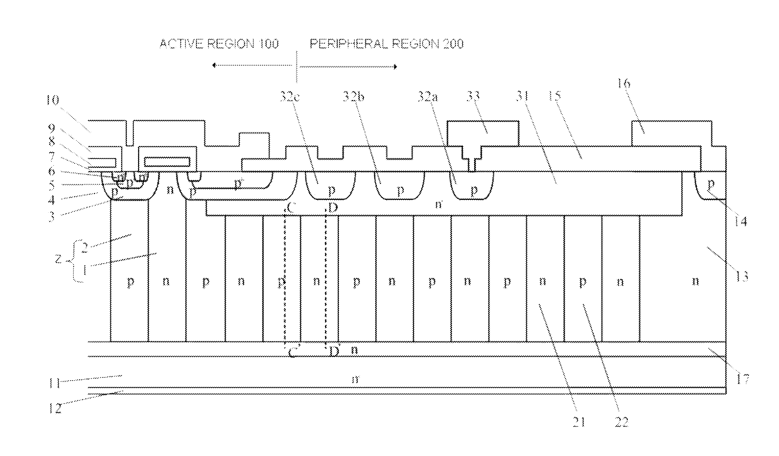
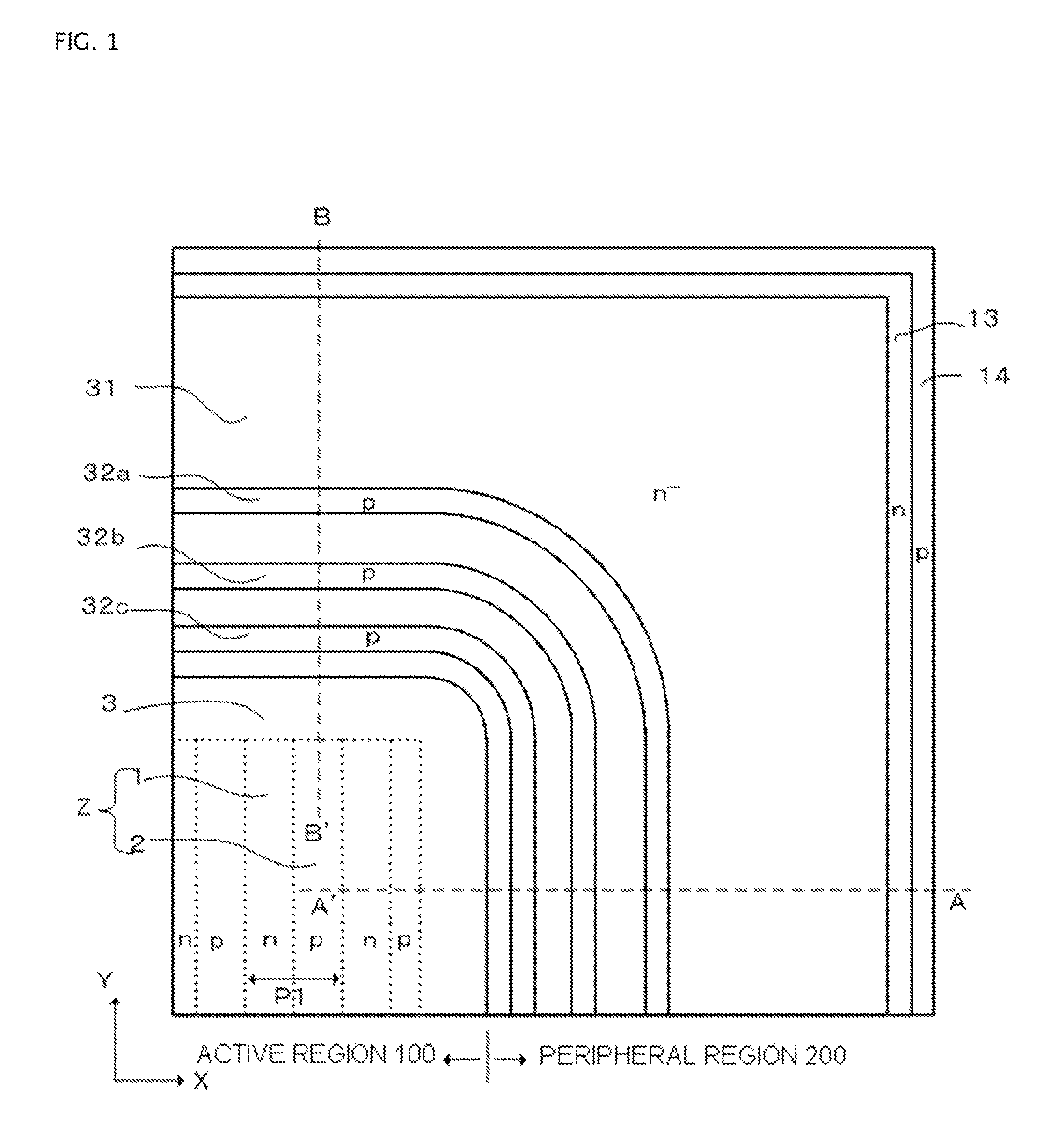
[0034]FIGS. 1 and 2 are one quarter plan views of a vertical superjunction MOSFET according to Embodiment 1. In FIG. 1, for ease of understanding, parallel pn layers Z, n-type surface region 31, and n-type channel stopper region 13 of the outermost surface, and p-base region 3 and p-type guard rings 32a, 32b, and 32c of the outermost periphery of active region 100, are shown. Rectangular regions indicated by the dotted lines in p-base region 3 show the parallel pn layers Z below p-base region 3. Surface n-type drift layer 4, p+ contact region 5, n-type source region 6, gate insulating film 7, gate electrode 8, interlayer insulating film 9, source electrode 10, field insulating film 15, channel stopper electrode 16, field plate 33, and the like, are not shown in FIG. 1. These are shown in FIG. 3. Also, high concentration semiconductor substrate 11, n-type buffer layer 17 formed by epitaxial growth with a uniform impurity concentration on the front surface of high concentration semico...

embodiment 2

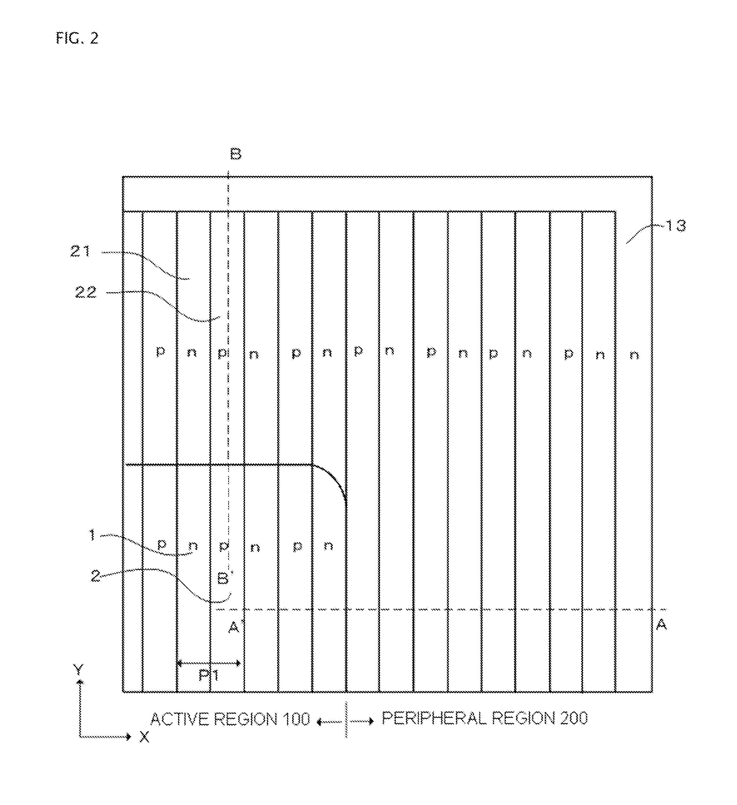
[0040]A superjunction MOSFET according to Embodiment 2 is shown in FIGS. 8, 9, 10, and 11. FIGS. 8 and 9 show, respectively, a plan view of the superjunction MOSFET and one portion (a quarter) of a sectional view in the vicinity of a half of the depth of the parallel pn layers. FIGS. 10 and 11 are sectional views cut along the line A-A′ and B-B′ in FIGS. 8 and 9, respectively. In FIG. 8, in the same way as in FIG. 1, one portion of the surface portions is omitted for ease of understanding. The differences between Embodiment 1 and Embodiment 2 are that the pitch of the parallel pn layers in peripheral region 200 is smaller than that of the parallel pn layers in active region 100, and the orientation of the stripes of the parallel pn layers in peripheral region 200, with the smaller pitch, that encloses the parallel pn layers in active region 100 is perpendicular to the that of the parallel pn layers in active region 100, and each conductive field plate 33 is connected to p-type guard...


PUM


Abstract

A semiconductor device is disclosed wherein a peripheral region with a high breakdown voltage and high robustness against induced surface charge is manufactured using a process with high mass productivity. The device has n-type drift region and p-type partition region of layer-shape deposited in a vertical direction to one main surface of n-type semiconductor substrate with high impurity concentration form as drift layer, alternately adjacent parallel pn layers in a direction along one main surface. Active region through which current flows and peripheral region enclosing the active region include parallel pn layers. P-type partition region has impurity concentration distribution where concentration decreases from surface toward substrate side, n-type surface region disposed on parallel pn layers in peripheral region, p-type guard rings disposed separately from each other on n-type surface region, and field plate disposed on inner and outer circumferential sides of p-type guard rings, and electrically connected.

Description

BACKGROUND OF THE INVENTION[0001]A. Field of the Invention[0002]The present invention relates to a superjunction semiconductor device with a high breakdown voltage and high current capacity applicable to a MOSFET (metal oxide semiconductor field effect transistor), IGBT (insulated gate bipolar transistor), bipolar transistor, or the like, and to a manufacturing method of the device. In the following description, the superjunction semiconductor device refers to a semiconductor device wherein a drift layer, in which a p-type region and n-type region of a column-shape or layer-shape deposited in a vertical direction to a main surface of a semiconductor substrate form alternately adjacent parallel pn layers in a direction along the main surface, has a function to flow a current in an “on” state and to hold a breakdown voltage in an “off” state.[0003]B. Description of the Related Art[0004]In general, semiconductor devices are classified into a lateral semiconductor device that has an ele...

Claims


Application Information

Patent Timeline
IPC IPC(8): H01L29/78
CPCH01L29/0619H01L29/0634H01L2924/1305H01L2924/1306H01L2924/13091H01L2924/13055H01L24/05H01L29/7811H01L29/404H01L29/0638H01L29/0696H01L29/0878H01L2924/00H01L2924/12036
Inventor ONISHI, YASUHIKO
Owner FUJI ELECTRIC CO LTD
Why Eureka
Try Eureka