

Light-emitting element unit and display device
a technology of light-emitting elements and display devices, which is applied in semiconductor devices, optics, instruments, etc., can solve the problems of low color reproducibility, low color purity of light emitted from display devices, and low color purity of green light transmitted through color filters, so as to improve the color reproducibility of display devices and increase the color purity of light. , the effect of high color purity
- Summary
- Abstract
- Description
- Claims
- Application Information
AI Technical Summary
Benefits of technology
Problems solved by technology
Method used
Image

Examples
embodiment 1
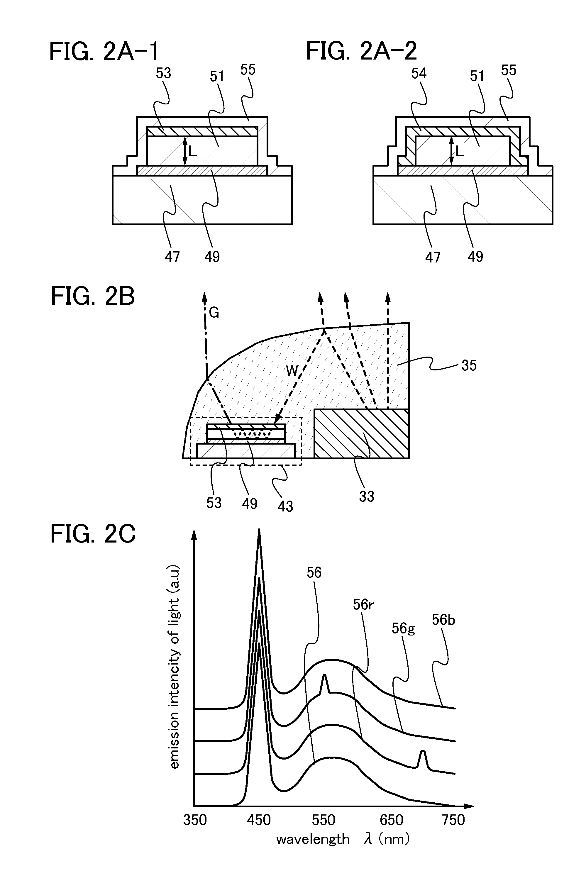
[0033]In this embodiment, an LED unit and a backlight which consume less power will be described with reference to FIGS. 1A and 1B and FIGS. 2A-1, 2A-2, 2B, and 2C.
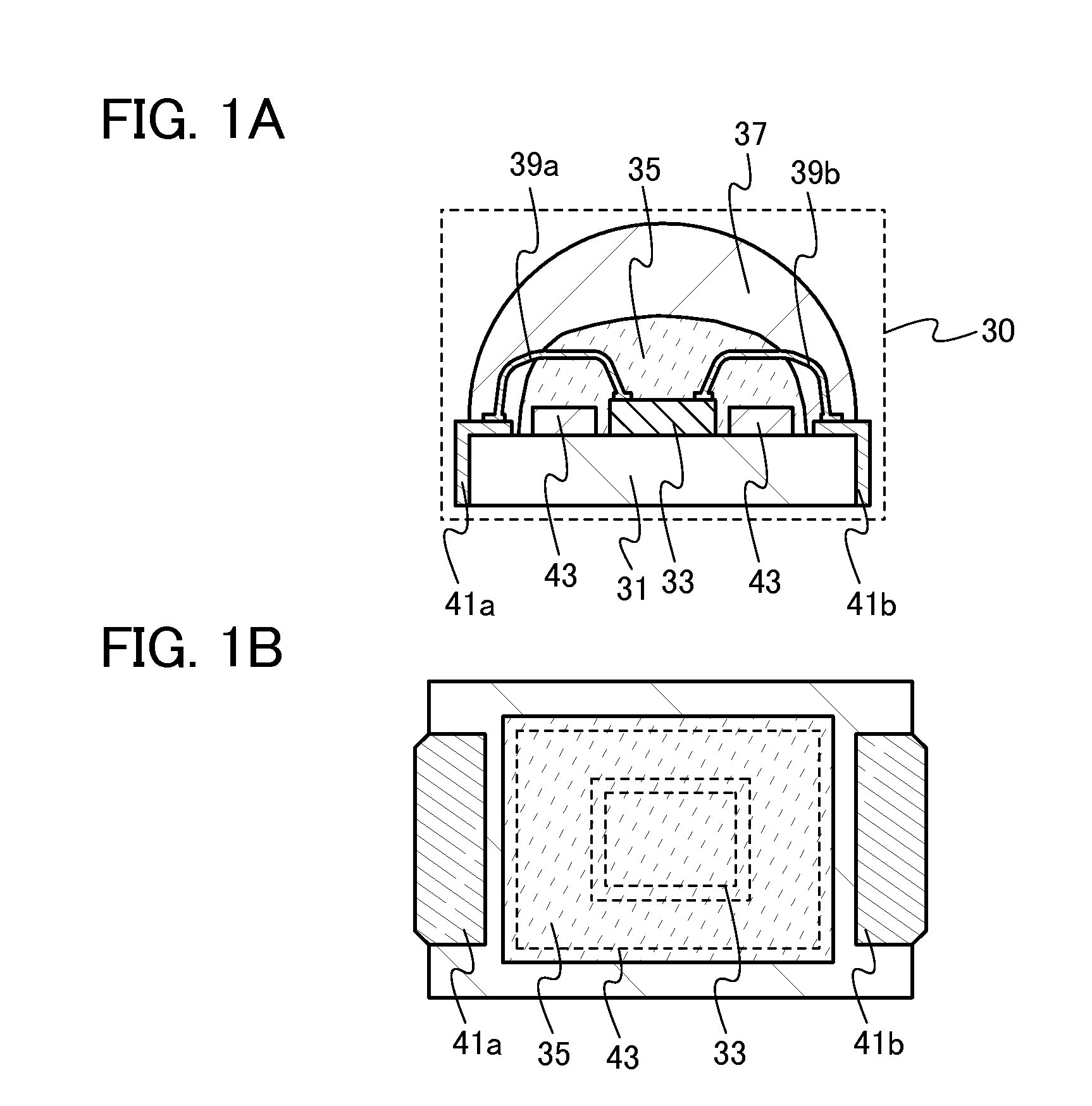
[0034]FIG 1A is a cross-sectional view of an LED unit 30.
[0035]The LED unit 30 includes a light-emitting element chip (hereinafter, referred to as an LED chip 33) provided over a wiring board 31, a phosphor layer 35 provided over the LED chip 33, and a light-transmitting convex organic resin layer 37 provided to cover the wiring board 31 and the phosphor layer 35. An electrode of the LED chip 33 is electrically connected to terminals 41a and 41b provided on side walls of the wiring board 31 through wirings 39a and 39b.
[0036]FIG. 1B is a top view of the LED chip 33 illustrated in FIG. 1A from which the light-transmitting convex organic resin layer 37 is excluded. As illustrated in FIG. 1B, there is a feature in that a micro optical resonator 43 is provided around the LED chip 33. The micro optical resonator 43 is an eleme...
embodiment 2
[0086]In this embodiment, a liquid crystal display device including the backlight module described in Embodiment 1 will be described.
[0087]The liquid crystal display device in this embodiment can be implemented for both passive matrix type and active matrix type. FIG. 6A is a block diagram illustrating a structure of an active-matrix liquid crystal display device 200.
[0088]In FIG. 6A, the liquid crystal display device 200 includes a pixel portion 210 which displays an image, a signal line driver circuit 214, a scan line driver circuit 211, a backlight module 40 which emits light to the pixel portion 210, and an LED control circuit 212 which controls a signal sent to an LED unit included in the backlight module 40. In addition, a circuit which is necessary for operating the liquid crystal display device, such as an image processing circuit (an image engine or the like) is included. All of them are provided for the control circuit board described in Embodiment 1. Note that the driver ...
embodiment 3
[0152]In this embodiment, a display device which controls the amount of light, in each pixel, transmitted from a backlight with use of micro electro mechanical systems (MEMS) will be described with reference to FIG. 12, FIG. 13, and FIG. 14.
[0153]FIG. 12 is a cross-sectional view of a display device 500 which controls the amount of light, in each pixel, transmitted from a backlight with use of MEMS having a three-dimensional structure and a microstructure part of which can be moved.
[0154]A reflective layer 503 is formed over a first substrate 501. A light-transmitting insulating layer 505 is provided over the reflective layer 503. MEMS switches 507r, 507g, and 507b are formed over the light-transmitting insulating layer 505. Note that although not illustrated, the light-transmitting insulating layer 505 includes a plurality of insulating layers, and transistors connected to the MEMS switches 507r, 507g, and 507b are formed between the insulating layers. As the transistors, the trans...
PUM
| Property | Measurement | Unit |
|---|---|---|
| wavelength | aaaaa | aaaaa |
| wavelength | aaaaa | aaaaa |
| wavelength range | aaaaa | aaaaa |
Abstract
Description
Claims
Application Information