Semiconductor memory device and driving method of semiconductor memory device

a memory device and semiconductor technology, applied in the field of memory devices, can solve the problems of tens of seconds, data loss within a relatively short time, and high power consumption even in a standby period, and achieve the effect of reducing the number of necessary wirings and reducing the area occupied by wirings

Inactive Publication Date: 2012-05-10
SEMICON ENERGY LAB CO LTD
View PDF7 Cites 26 Cited by
  • Summary
  • Abstract
  • Description
  • Claims
  • Application Information

AI Technical Summary

Benefits of technology

[0023]Note that a source of the reading transistor is supplied with an appropriate potential by another wiring. Depending on the reading method, a fluctuation in this potential can be small. For example, a driving method by which a constant potential can be held for 1 second or longer can be employed. Therefore, the resistance of the wiring connected to the source of the reading transistor does not necessarily need to be low. For example, silicon which is doped with impurities, or silicon which is doped with impurities and has a surface where silicide is formed may be used.
[0053]Further, as apparent from the above description, the number of transistors used in one memory cell is three or less, typically two. These are provided in different layers, whereby the area occupied by the memory cells can be reduced. Furthermore, as described above, the wirings are arranged so as to have a three-dimensional structure or the wiring is shared by different elements, whereby the number of wirings can be reduced. Consequently, the degree of integration can be further increased.

Problems solved by technology

However, even when a transistor used for switching is in an off state, a slight amount of leakage current is generated between a source and a drain; thus, the data is lost within a relatively short time (several tens of seconds at the longest).
Therefore, the data needs to be rewritten (refreshed) on a regular cycle (generally once every several tens of milliseconds), and power consumption is high even in a standby period.
In addition, data can be held for an extremely long period without refresh operation.

Method used


Image

  • Semiconductor memory device and driving method of semiconductor memory device
  • Semiconductor memory device and driving method of semiconductor memory device
  • Semiconductor memory device and driving method of semiconductor memory device

Examples


embodiment 1

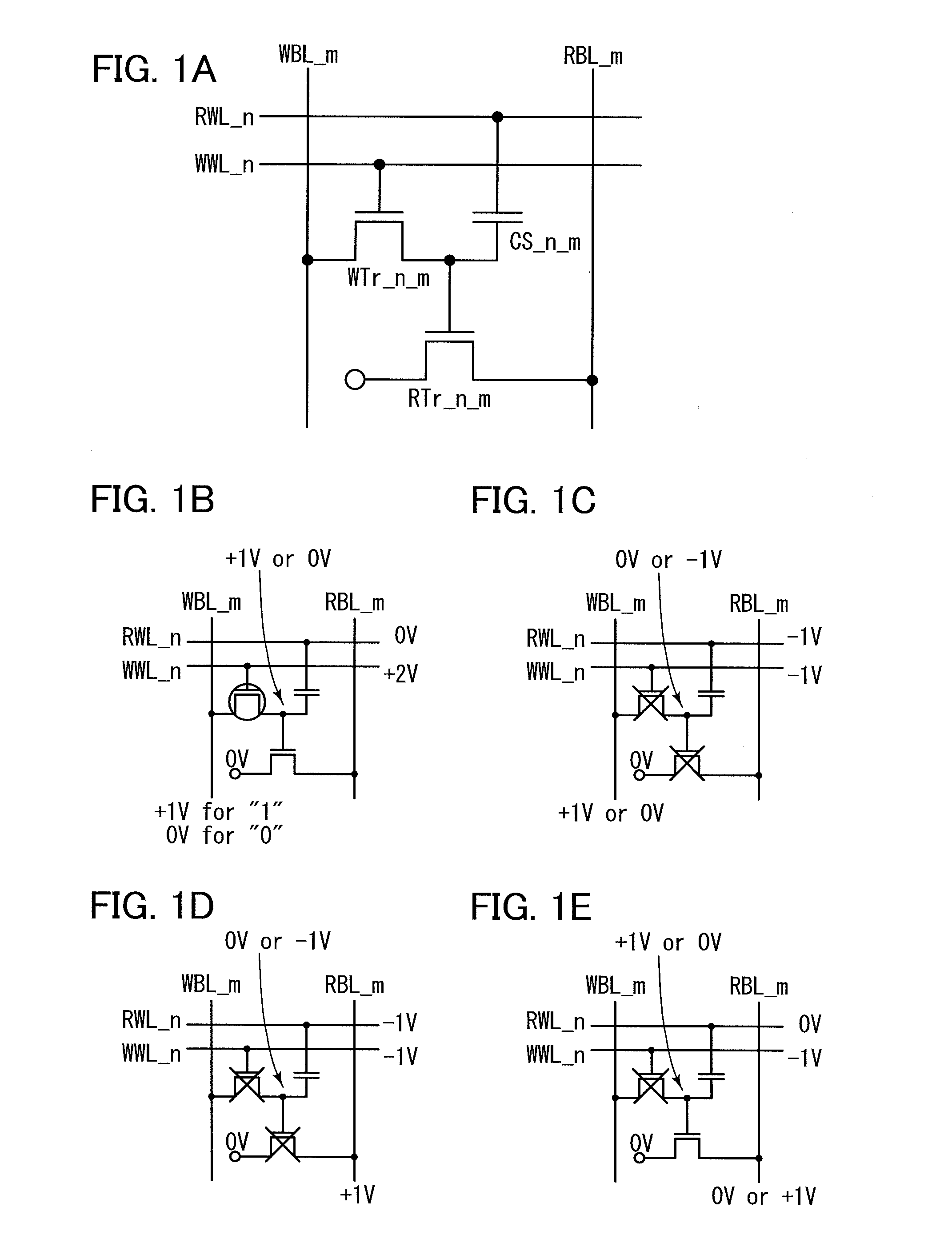
[0068]FIG. 1A illustrates a memory cell of this embodiment. Here, n and m are natural numbers of 1 or more. In FIG. 1A, a memory cell including a writing transistor WTr_n_m, a reading transistor RTr_n_m, and a capacitor CS_n_m is illustrated. Here, a source of the writing transistor WTr_n_m is connected to a gate of the reading transistor RTr_n_m and one electrode of the capacitor CS_n_m.

[0069]In the memory cell illustrated in FIG. 1A, the writing transistor WTr_n_m and the reading transistor RTr_n_m are each an n-channel transistor; however, without limitation to this, the following structures can be employed, for example: the writing transistor WTr_n_m and the reading transistor RTr_n_m are each a p-channel transistor; the writing transistor WTr_n_m and the reading transistor RTr_n_m are an n-channel transistor and a p-channel transistor, respectively; and the writing transistor WTr_n_m and the reading transistor RTr_n_m are a p-channel transistor and an n-channel transistor, resp...

embodiment 2

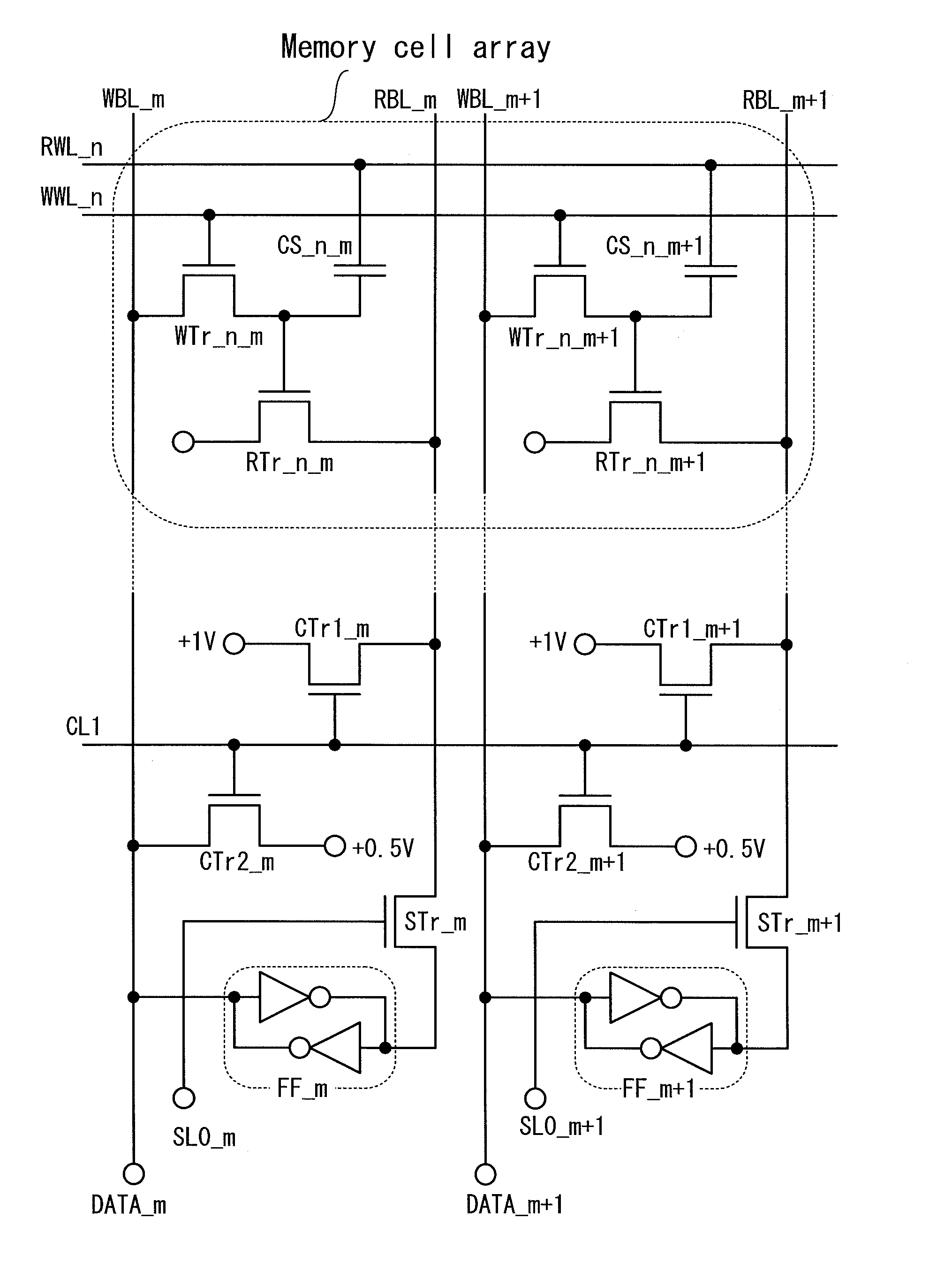
[0103]FIG. 4 is a circuit diagram illustrating part of a memory cell array of a semiconductor memory device in this embodiment, and FIG. 5 is a circuit diagram illustrating part of a driver circuit of a semiconductor memory device in this embodiment. FIGS. 9A to 9E illustrate an example of a driving method of a semiconductor memory device in this embodiment.

[0104]In the semiconductor memory device in this embodiment, as illustrated in FIG. 4, a plurality of memory cells including a memory cell in the (n−1)-th row and the m-th column, a memory cell in the n-th row and the (m−1)-th column, and the like are arranged in a matrix. Here, n and m are each an even number of 2 or more.

[0105]In the memory cell in the n-th row and the (m−1)-th column, a source of a writing transistor WTr_n_m−1, a gate of a reading transistor RTr_n_m−1, and one electrode of a capacitor CS_n_m−1 are connected to each other. In the memory cell in the (n−1)-th row and the m-th column, a source of a writing transis...

embodiment 3

[0130]In this embodiment, examples of a layout and a manufacturing method of the semiconductor memory device described in Embodiment 2 will be described with reference to FIGS. 6A to 6D, FIGS. 7A to 7C, and FIGS. 8A to 8F. FIGS. 6A to 6D and FIGS. 7A to 7C are cross-sectional views illustrating a manufacturing process, and FIGS. 8A to 8F illustrate a layout of components such as main wirings and the like in main layers. Note that line A-B denotes the same position through FIGS. 8A to 8F. Further, dotted lines in FIGS. 8A to 8F denote coordinates, and can be used as reference when a positional relationship between structures in different layers is referred to.

[0131]FIG. 8A illustrates shapes of element isolation insulators 102 provided over a semiconductor substrate. The element isolation insulators 102 have a C-like shape. A continuous region 101a is formed in a direction intersecting with line A-B in the drawing, and this region is to be an impurity region 104a functioning as a wir...


PUM

PropertyMeasurementUnit
capacitanceaaaaaaaaaa
aspect ratioaaaaaaaaaa
currentaaaaaaaaaa

Abstract

A novel semiconductor memory device whose power consumption is low is provided. A source of a writing transistor WTr_n_m, a gate of a reading transistor RTr_n_m, and one electrode of a capacitor CS_n_m are connected to each other. A gate and a drain of the writing transistor WTr_n_m are connected to a writing word line WWL_n and a writing bit line WBL_m, respectively. The other electrode of the capacitor CS_n_m is connected to a reading word line RWL_n. A drain of the reading transistor RTr_n_m is connected to a reading bit line RBL_m. Here, the potential of the reading bit line RBL_m is input to an inverting amplifier circuit such as a flip-flop circuit FF_m to be inverted by the inverting amplifier circuit. This inverted potential is output to the writing bit line WBL_m.

Description

BACKGROUND OF THE INVENTION[0001]1. Field of the Invention[0002]The present invention relates to a memory device including a semiconductor.[0003]2. Description of the Related Art[0004]As a memory device including a semiconductor, which is used in various electronic products and electronics products, a dynamic random access memory (DRAM), a static random access memory (SRAM), and the like can be given.[0005]In a DRAM, data is stored by holding charge in a capacitor which is provided in a memory cell. However, even when a transistor used for switching is in an off state, a slight amount of leakage current is generated between a source and a drain; thus, the data is lost within a relatively short time (several tens of seconds at the longest). Therefore, the data needs to be rewritten (refreshed) on a regular cycle (generally once every several tens of milliseconds), and power consumption is high even in a standby period.[0006]While miniaturization of a circuit has been attempted, a dee...

Claims


Application Information

Patent Timeline
Patent Type & Authority Applications(United States)
IPC IPC(8): G11C11/24
CPCG11C11/404G11C11/405G11C16/02G11C11/40G11C7/1078G11C11/24G11C7/1048
Inventor TAKEMURA, YASUHIKO
Owner SEMICON ENERGY LAB CO LTD
Why Eureka
Try Eureka