Substrate processing apparatus, method of manufacturing semiconductor device and semiconductor device

a processing apparatus and semiconductor technology, applied in the direction of chemical vapor deposition coating, coating, basic electric elements, etc., can solve the problems of clogging the nozzle, reducing the performance of high-k films, and reducing the permittivity of films or increasing leak curren

Active Publication Date: 2012-05-17
KOKUSA ELECTRIC CO LTD
View PDF2 Cites 337 Cited by
  • Summary
  • Abstract
  • Description
  • Claims
  • Application Information

AI Technical Summary

Benefits of technology

[0009]However, when a process temperature becomes high, the inside of a nozzle reaches a high temperature and high pressure state, and a source gas may be pyrolyzed in the nozzle. For example, when TMA gas is used as a source gas, reaction products may be formed by a chemical vapor deposition (CVD) reaction between aluminum (Al) atoms in the nozzle. Otherwise, the reaction products or decomposed matters of the TMA gas may be accumulated on an inner wall of the nozzle, clogging the nozzle. In addition, as foreign substances generated by separation of the reaction products or the decomposed matters from the inner wall of the nozzle are scattered in the process chamber to be stuck to the substrate, substrate processing quality may be decreased.
[0010]In order to solve these problems, an object of the present invention is to provide a substrate processing apparatus and a method of manufacturing a semiconductor device that are capable of suppressing accumulation of reaction products or decomposed matters on an inner wall of a nozzle and suppressing foreign substances from being scattered in a process chamber. In addition, another object of the present invention is to provide a semiconductor device having a high-quality thin film with minute introduction of the foreign substances through the substrate processing apparatus and the method of manufacturing the semiconductor device.
[0011]According to an aspect of the present invention, there is provided a substrate processing apparatus including: a process chamber configured to accommodate therein a plurality of substrates stacked horizontally; a heating unit installed outside the process chamber and configured to heat an inside of the process chamber; a source gas supply unit configured to supply a first process gas; a source gas nozzle connected to the source gas supply unit and configured to supply the first process gas supplied from the source gas supply unit into the process chamber; an exhaust unit configured to exhaust the inside of the process chamber in a substantially horizontal direction; and a control unit configured to control at least the heating unit, the source gas supply unit and the exhaust unit, wherein the source gas nozzle is disposed in a region in the process chamber where the first process gas is not decomposed even when an inside temperature of the process chamber is higher than a pyrolysis temperature of the first process gas, and the control unit controls the source gas supply unit to supply the first process gas into the process chamber at least two times at different flow velocities such that the first process gas is prevented from being mixed.
[0015]According to the present invention, accumulation of reaction products or decomposed matters on an inner wall of a nozzle can be suppressed, and scattering of foreign substances in a process chamber can be suppressed. In addition, sticking of the foreign substances to a substrate can be suppressed to avoid a decrease in substrate processing quality.

Problems solved by technology

ALD using TMA gas and ozone gas may be performed at a temperature in a process chamber set to 200° C. to 400° C. However, at such a process temperature, carbon (C) atoms and hydrogen (H) atoms constituting a source gas or a reactive gas may remain in a film as impurities, causing a decrease in performance of a high-k film, for example, a decrease in permittivity of the film or an increase in leak current.
However, when a process temperature becomes high, the inside of a nozzle reaches a high temperature and high pressure state, and a source gas may be pyrolyzed in the nozzle.
Otherwise, the reaction products or decomposed matters of the TMA gas may be accumulated on an inner wall of the nozzle, clogging the nozzle.
In addition, as foreign substances generated by separation of the reaction products or the decomposed matters from the inner wall of the nozzle are scattered in the process chamber to be stuck to the substrate, substrate processing quality may be decreased.

Method used


Image

  • Substrate processing apparatus, method of manufacturing semiconductor device and semiconductor device
  • Substrate processing apparatus, method of manufacturing semiconductor device and semiconductor device
  • Substrate processing apparatus, method of manufacturing semiconductor device and semiconductor device

Examples


first embodiment

of the Invention

[0036](1) Configuration of Substrate Processing Apparatus

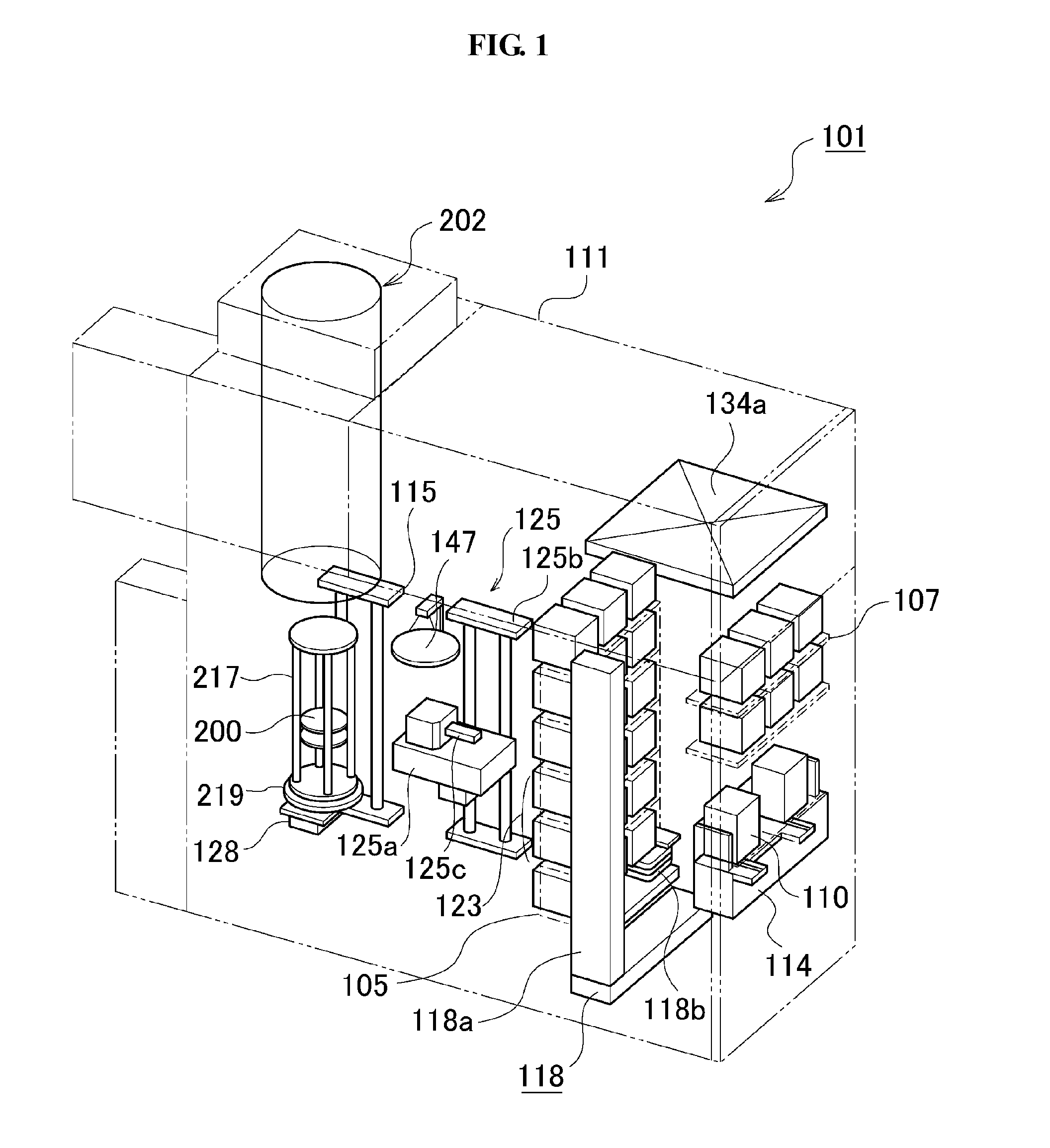
[0037]First, a configuration example of a substrate processing apparatus 101 in accordance with an embodiment of the present invention will be described with reference to FIGS. 1 and 5.

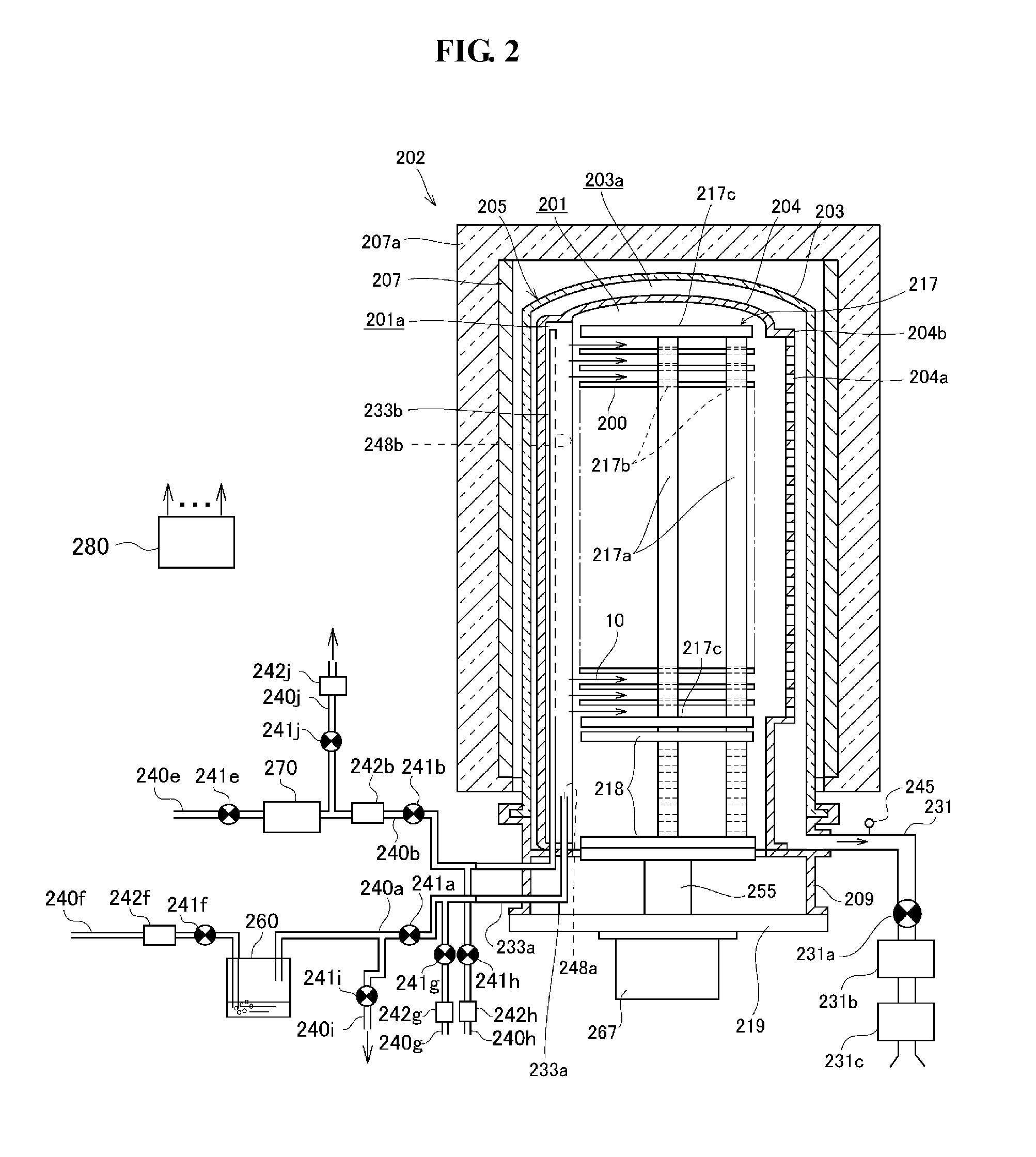
[0038]FIG. 1 is a schematic configuration view of a substrate processing apparatus 101 in accordance with an embodiment of the present invention. FIG. 5 is a schematic view showing a gas flow generated in a process tube installed at the substrate processing apparatus in accordance with an embodiment of the present invention.

[0039]As shown in FIG. 1, the substrate processing apparatus 101 in accordance with the embodiment includes a housing 111. In order to convey a wafer 200, which is a substrate formed of silicon, into / from the housing 111, a cassette 110, which is a wafer carrier (a substrate receiving vessel) for receiving a plurality of wafers 200, is used. A cassette stage (a substrate receiving vessel delivery platform) 114...

second embodiment

of the Invention

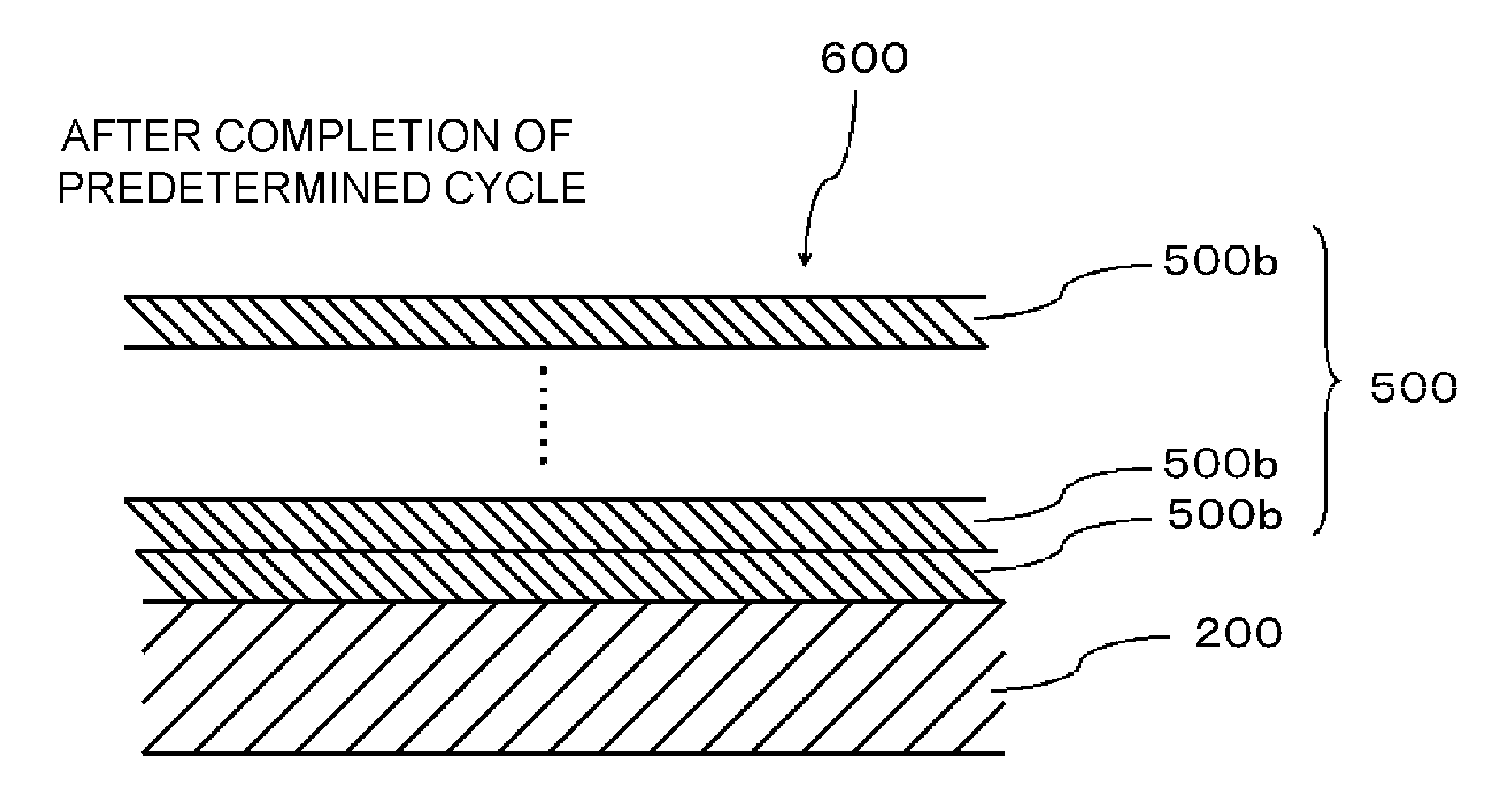
[0151]In the first embodiment, the source gas nozzle 233a was constituted by a short nozzle in which a vertical portion was disposed lower than the region in which the wafer 200 was to be accommodated, not the porous long nozzle like the reactive gas nozzle 233b. However, when the source gas nozzle 233a is constituted by the short nozzle, while pyrolysis of the source gas in the source gas nozzle 233 can be suppressed, a supply amount of the TMA gas may be locally uneven in the process chamber 201 (between the wafers 200). For example, the supply amount of the TMA gas to the wafer 200 at each cycle may be increased at the wafer 200 at an upper side in the process chamber 201 and decreased at the wafer 200 at a lower side therein. As a result, a film thickness of the aluminum oxide film 500 formed on the wafer 200 may be uneven between the wafers 200.

[0152]A difference in film thickness between the wafers 200 is likely to increase particularly when the processing temp...

third embodiment

of the Invention

[0209]Next, the third embodiment of the present invention will be described. The third embodiment is distinguished from the second embodiment in that after supplying the TMA gas into the process chamber 201 at the first flow velocity and before supplying the TMA gas into the process chamber 201 at the second flow velocity, the supply of the ozone gas in the process chamber 201 is performed. That is, in this embodiment, whenever the TMA gas is supplied into the process chamber 201 at different flow velocities, the ozone gas is supplied into the process chamber 201 to oxidize the Al-containing layer 500a on the wafer 200. The embodiment is particularly effective when the reactive gas has a property of being easily pyrolyzed. That is, the embodiment is particularly effective when the reactive gas nozzle 233b is constituted as a short nozzle similar to the source gas nozzle 233a. That is, hereinafter, overlapping description with the first and second embodiments will be ...


PUM

PropertyMeasurementUnit
temperatureaaaaaaaaaa
timeaaaaaaaaaa
temperatureaaaaaaaaaa

Abstract

Provided is a substrate processing apparatus capable of suppressing accumulation of reaction products or decomposed matters on an inner wall of a nozzle and suppressing scattering of foreign substances in a process chamber. The substrate processing apparatus includes a process chamber, a heating unit, a source gas supply unit, a source gas nozzle, an exhaust unit, and a control unit configured to control at least the heating unit, the source gas supply unit and the exhaust unit. The source gas nozzle is disposed at a region in the process chamber, in which a first process gas is not decomposed even under a temperature in the process chamber higher than a pyrolysis temperature of the first process gas, and the control unit supplies the first process gas into the process chamber two or more times at different flow velocities to prevent the first process gas from being mixed.

Description

CROSS-REFERENCE TO RELATED PATENT APPLICATION[0001]This U.S. non-provisional patent application claims priority under 35 U.S.C. §119 of Japanese Patent Application No. 2010-253231, filed on Nov. 11, 2010, in the Japanese Patent Office, the entire contents of which are hereby incorporated by reference.BACKGROUND OF THE INVENTION[0002]1. Field of the Invention[0003]The present invention relates to a substrate processing apparatus, a method of manufacturing a semiconductor device, and a semiconductor device.[0004]2. Description of the Related Art[0005]In atomic layer deposition (ALD), for example, a source gas, which is a source material of a film, and a reactive gas, which reacts with the source gas, are alternately supplied into a process chamber so that a thin film is sequentially deposited by one atomic layer, forming a predetermined film on a substrate. The film formed by the ALD may be, for example, an aluminum oxide film (AlO film) formed by trimethylaluminum (TMA) gas, which is...

Claims


Application Information

Patent Timeline
Patent Type & Authority Applications(United States)
IPC IPC(8): H01L23/58H01L21/31C23C16/52
CPCC23C16/403C23C16/45527H01L21/0228C23C16/45578H01L21/02178C23C16/45546C23C16/455H01L21/31
Inventor SASAKI, SHINYATAKEBAYASHI, YUJIKOGURA, SHINTARO
Owner KOKUSA ELECTRIC CO LTD
Why Eureka
Try Eureka