Photoresist composition for negative development and pattern forming method using thereof

a technology of composition and composition, applied in the field of photolithography, can solve the problems of becoming ever more difficult to print small features, and achieve the effect of negative developmen

Inactive Publication Date: 2012-05-17
GLOBALFOUNDRIES INC
View PDF13 Cites 11 Cited by
  • Summary
  • Abstract
  • Description
  • Claims
  • Application Information

AI Technical Summary

Benefits of technology

[0006]The present invention provides a photoresist composition which is capable of negative development using an organic solvent d

Problems solved by technology

However, as semiconductor ground rule gets smaller, it has become ever more challenging to print small features such as trenches and vias of small dimensions using traditional positive resist with aqueous base developer due to the poor optical image contrast of the dark field masks used to create the trenches and vias.

Method used


Image

  • Photoresist composition for negative development and pattern forming method using thereof
  • Photoresist composition for negative development and pattern forming method using thereof
  • Photoresist composition for negative development and pattern forming method using thereof

Examples


example 1

Resist A Formulation

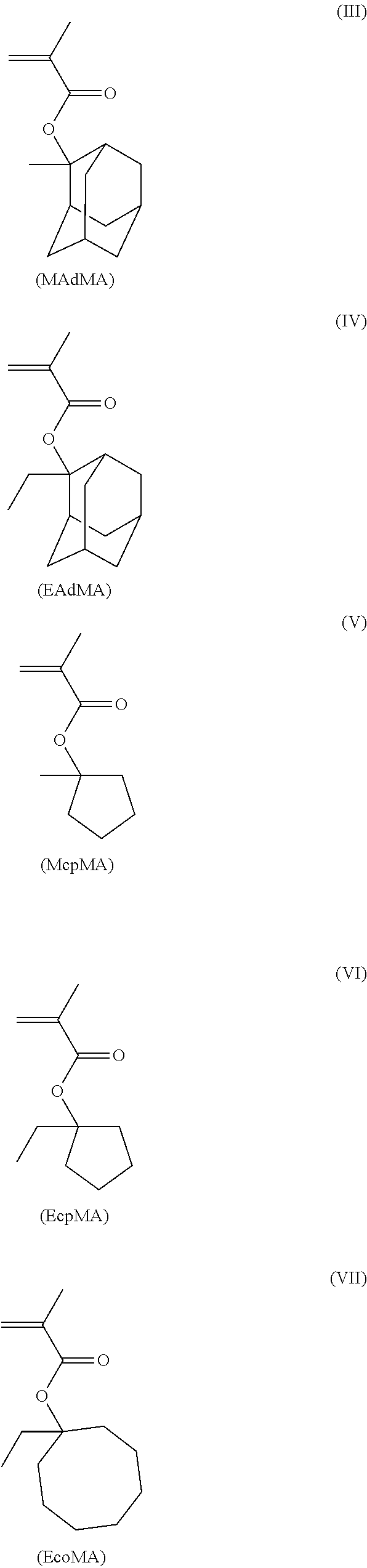
[0050]A tetrapolymer consisting of 10 mole % McpMA, 40 mole % MAdMA, 15 mole % HAdMA and 35 mole % NLM was dissolved in PGMEA with 30 wt % GBL(γ-butyrolactone), 2 wt % triphenyl-sulfonium 2-bicyclo[2.2.1]hept-7-yl-1,1,2,2-tetrafluoro-ethanesulfonate, 5 wt % (4-cyclohexyl-phenyl)-diphenyl-sulfonium 1,1,2,2,3,3,4,4,4-nonafluoro-butane-1-sulfonate and 0.69 wt % of 2-hydroxymethyl-pyrrolidine-1-carboxylic acid tert-butyl ester (all wt % are relative to the polymer) to make a solution with 4 wt % of solid content. The resulting solution was filtered through a 0.2 μm filter. The resist was spin-coated on a 12″ silicon wafer which consists of 42 nm thickness coating of Dow Chemical AR40 anti-reflective layer on top of LTO (low temperature oxide) and SiCOH (low k dielectric). The resist was post-applying baked (PAB) at 110° C. for 60 seconds and exposed to 193 nm wavelength light on an ASML stepper (0.93 NA, 0.84 outer and 0.59 inner a annular illumination). The wafer wa...

example 2

Resist B Formulation

[0051]A tetrapolymer consisting of 10 mole % McpMA, 40 mole % MAdMA, 15 mole % HEAdMA and 35 mole % NLM was dissolved in PGMEA with 30 wt % GBL, 5 wt % triphenyl-sulfonium 1,1,2,2,3,3,4,4,4-nonafluoro-butane-1-sulfonate and 0.33 wt % of piperidine-1-carboxylic acid tert-butyl ester (all wt % are relative to the polymer) to make a solution with 4 wt % of solid content. The resulting solution was filtered through a 0.2 μm filter. The resist was spin-coated on a 12″ silicon wafer which consists of 42 nm thickness coating of Dow Chemical AR40 anti-reflective layer on top of LTO (low temperature oxide) and SiCOH (low k dielectric). The resist was post-applying baked (PAB) at 110° C. for 60 seconds and exposed to 193 nm wavelength light on an ASML stepper (0.93 NA, 0.84 outer and 0.59 inner σ annular illumination). The wafer was then post-exposure baked (PEB) at 120° C. for 60 seconds. It was developed using a single puddle develop process for 30 seconds with PGMEA as ...

example 3

Resist C Formulation

[0052]A copolymer consisting of 50 mole % MAdMA and 50 mole % GMA was dissolved in PGMEA with 30 wt % GBL, 7 wt % triphenyl-sulfonium 1,1,2,2,3,3,4,4,4-nonafluoro-butane-1-sulfonate and 0.82 wt % of piperidine-1-carboxylic acid tert-butyl ester (all wt % are relative to the polymer) to make a solution with 4 wt % of solid content. The resulting solution was filtered through a 0.2 μm filter. The resist was spin-coated on a 12″ silicon wafer which consists of 42 nm thickness coating of Dow Chemical AR40 anti-reflective layer on top of LTO (low temperature oxide) and SiCOH (low k dielectric). The resist was post-applying baked (PAB) at 110° C. for 60 seconds and exposed to 193 nm wavelength light on an ASML stepper (0.93 NA, 0.84 outer and 0.59 inner a annular illumination). The wafer was then post-exposure baked (PEB) at 110° C. for 60 seconds. It was developed using a single puddle develop process for 30 seconds with PGMEA solvent developer. Lithography resolution...


PUM


Abstract

The present invention relates to a photoresist composition capable of negative development and a pattern forming method using the photoresist composition. The photoresist composition includes an imaging polymer and a radiation sensitive acid generator. The imaging polymer includes a first monomeric unit having a pendant acid labile moiety and a second monomeric unit containing a reactive ether moiety, an isocyanide moiety or an isocyanate moiety. The patterning forming method utilizes an organic solvent developer to selectively remove unexposed regions of a photoresist layer of the photoresist composition to form a patterned structure in the photoresist layer. The photoresist composition and the pattern forming method are especially useful for forming material patterns on a semiconductor substrate using 193 nm (ArF) lithography.

Description

FIELD OF THE INVENTION[0001]This invention relates generally to photolithography, and more particularly to a photoresist composition capable of negative development using an organic solvent as the developer. This invention is also directed to a pattern forming method of using such a photoresist composition.BACKGROUND OF THE INVENTION[0002]Photolithography is a process which uses light to transfer a geometric pattern from a photomask to a substrate such as a silicon wafer. In a photolithography process, a photoresist layer is first formed on the substrate. The substrate is baked to remove any solvent remained in the photoresist layer. The photoresist is then exposed through a photomask with a desired pattern to a source of actinic radiation. The radiation exposure causes a chemical reaction in the exposed areas of the photoresist and creates a latent image corresponding to the mask pattern in the photoresist layer. The photoresist is next developed in a developer solution, usually an...

Claims


Application Information

Patent Timeline
IPC IPC(8): G03F7/004G03F7/20
CPCG03F7/0397G03F7/004G03F7/325
Inventor CHEN, KUANG-JUNGLIU, SENHUANG, WU-SONGLI, WAI-KIN
Owner GLOBALFOUNDRIES INC
Why Eureka
Try Eureka