System and Method for Step Coverage Measurement

Inactive Publication Date: 2012-05-17
INTERMOLECULAR
View PDF1 Cites 0 Cited by
  • Summary
  • Abstract
  • Description
  • Claims
  • Application Information

AI Technical Summary

Problems solved by technology

However, uniform processing across an entire substrate can be disadvantageous when optimizing, qualifying, or investigating new materials, new processes, and / or new process sequence integration schemes, since the entire substrate is nominally made the same using the same materials, processes, and process sequence integration schemes.
Thus, the full wafer uniform processing under conventional processing techniques results in fewer data points per substrate, longer times to accumulate a wide variety of data, and higher costs associated with obtaining such data.
Conventional techniques generally do not efficiently screen and analyze an array of materials, processes, and process sequence integration schemes across a substrate, and thus typically do not efficiently evaluate alternative materials, processes, and process sequence integration schemes for semiconductor manufacturing processes.

Method used


Image

  • System and Method for Step Coverage Measurement
  • System and Method for Step Coverage Measurement
  • System and Method for Step Coverage Measurement

Examples


Embodiment Construction

[0020]The embodiments herein and the various features and advantageous details thereof are explained more fully with reference to the non-limiting embodiments that are illustrated in the accompanying drawings and detailed in the following description. Descriptions of well-known components and processing techniques are omitted so as to not unnecessarily obscure the embodiments herein. The examples used herein are intended merely to facilitate an understanding of ways in which the embodiments herein may be practiced and to further enable those of skill in the art to practice the embodiments herein. Accordingly, the examples should not be construed as limiting the scope of the embodiments herein.

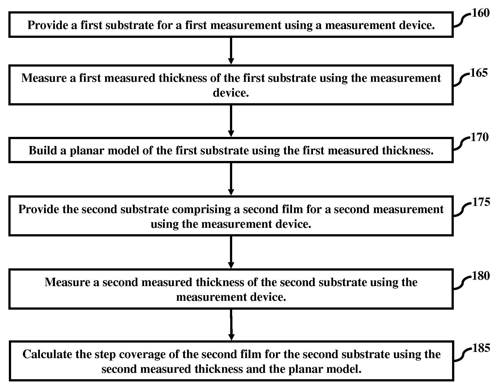
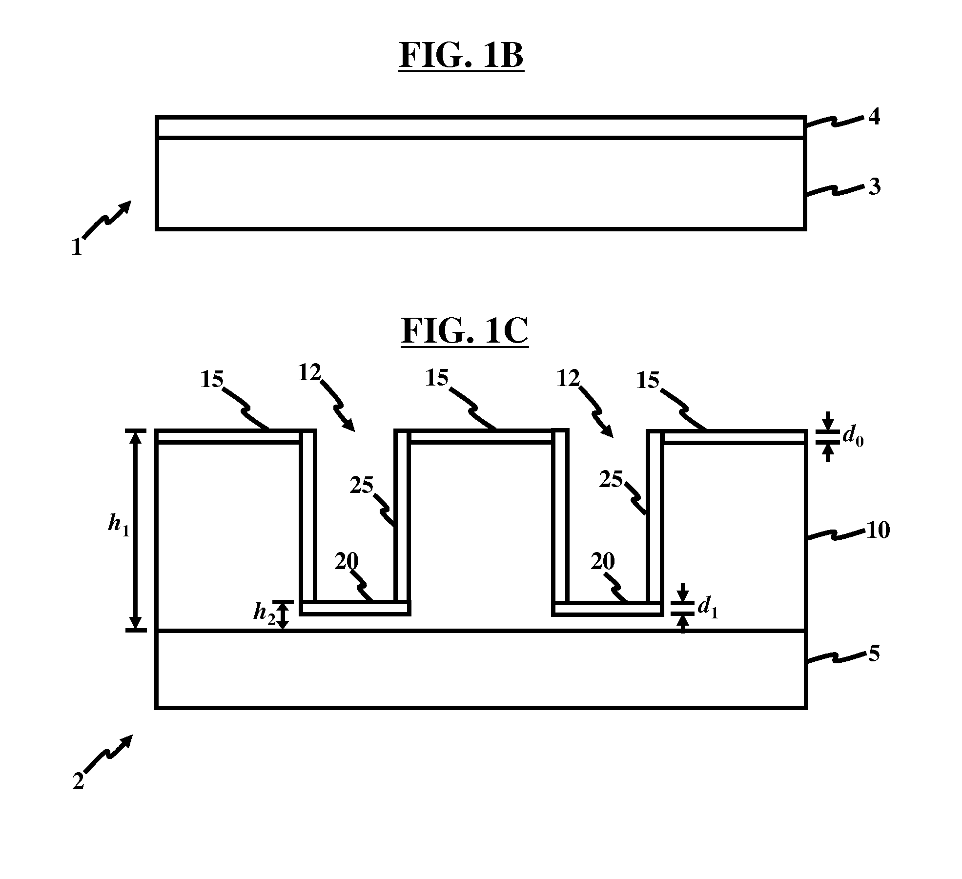
[0021]Referring now to the drawings, and more particularly to FIGS. 1A through 9, there are shown embodiments herein. The manufacturing of integrated circuits (IC) semiconductor devices, flat panel displays, optoelectronics devices, data storage devices, magneto electronic devices, magneto opti...


PUM


Abstract

Determining an unknown step coverage of a thin film deposited on a 3D wafer includes exposing a planar wafer comprising a first film deposited thereon to X-ray radiation to create first fluorescent radiation; detecting the first fluorescent radiation; measuring a number of XRF counts on the planar wafer; creating an XRF model of the planar wafer; providing a portion of the 3D wafer comprising troughs and a second film deposited thereon; determining a multiplier factor between the portion of the 3D wafer and the planar wafer; exposing the portion of the 3D wafer to X-ray radiation to create second fluorescent radiation; detecting the second fluorescent radiation; measuring a number of XRF counts on the portion of the 3D wafer; calculating a step coverage of the portion of the 3D wafer; and determining a uniformity of the 3D wafer based on the step coverage of the portion of the 3D wafer.

Description

BACKGROUND[0001]1. Technical Field[0002]The embodiments herein generally relate to semiconductor processing technologies, and more specifically, to a high throughput metrology method use to determine the coverage of a thin film over patterned features in semiconductor processing technologies.[0003]2. Description of the Related Art[0004]The ability to process uniformly across a monolithic substrate and / or across a series of monolithic substrates is advantageous for manufacturing efficiency and cost effectiveness, as well as repeatability and control. However, uniform processing across an entire substrate can be disadvantageous when optimizing, qualifying, or investigating new materials, new processes, and / or new process sequence integration schemes, since the entire substrate is nominally made the same using the same materials, processes, and process sequence integration schemes. Each processed substrate generally represents, in essence, only one possible variation per substrate. Thu...

Claims


Application Information

Patent Timeline
IPC IPC(8): G06F17/10
CPCG01N23/223H01L22/12
Inventor CHEN, HANHONGHAYWOOD, EDWARDKUMAR, PRAGATI
Owner INTERMOLECULAR
Why Eureka
Try Eureka