Current mode synchronous rectification dc/dc converter

Active Publication Date: 2012-05-24
ROHM CO LTD
View PDF0 Cites 21 Cited by
  • Summary
  • Abstract
  • Description
  • Claims
  • Application Information

AI Technical Summary

Benefits of technology

[0024]According to the present invention, a current mode synchronous rectification DC / DC converter capable of inhibiting fluctuations of an output voltage while starting can be provided.

Problems solved by technology

However, the conventional DC / DC converter has the following problem: in a period until a voltage value of a reference voltage REF reaches a stable action area i.e., a target value of an output voltage VO capable of stable output in a state of setting a power of a PWM signal (PWM) to a minimum value, an output voltage VO fluctuates (referring to FIG. 9).

Method used


Image

  • Current mode synchronous rectification dc/dc converter
  • Current mode synchronous rectification dc/dc converter
  • Current mode synchronous rectification dc/dc converter

Examples


first embodiment

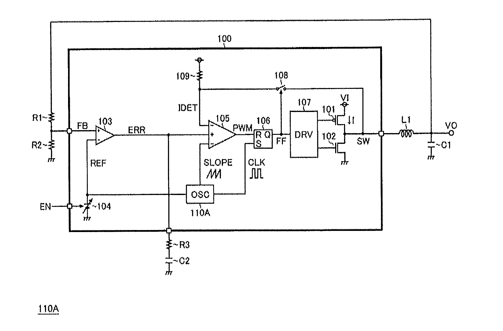
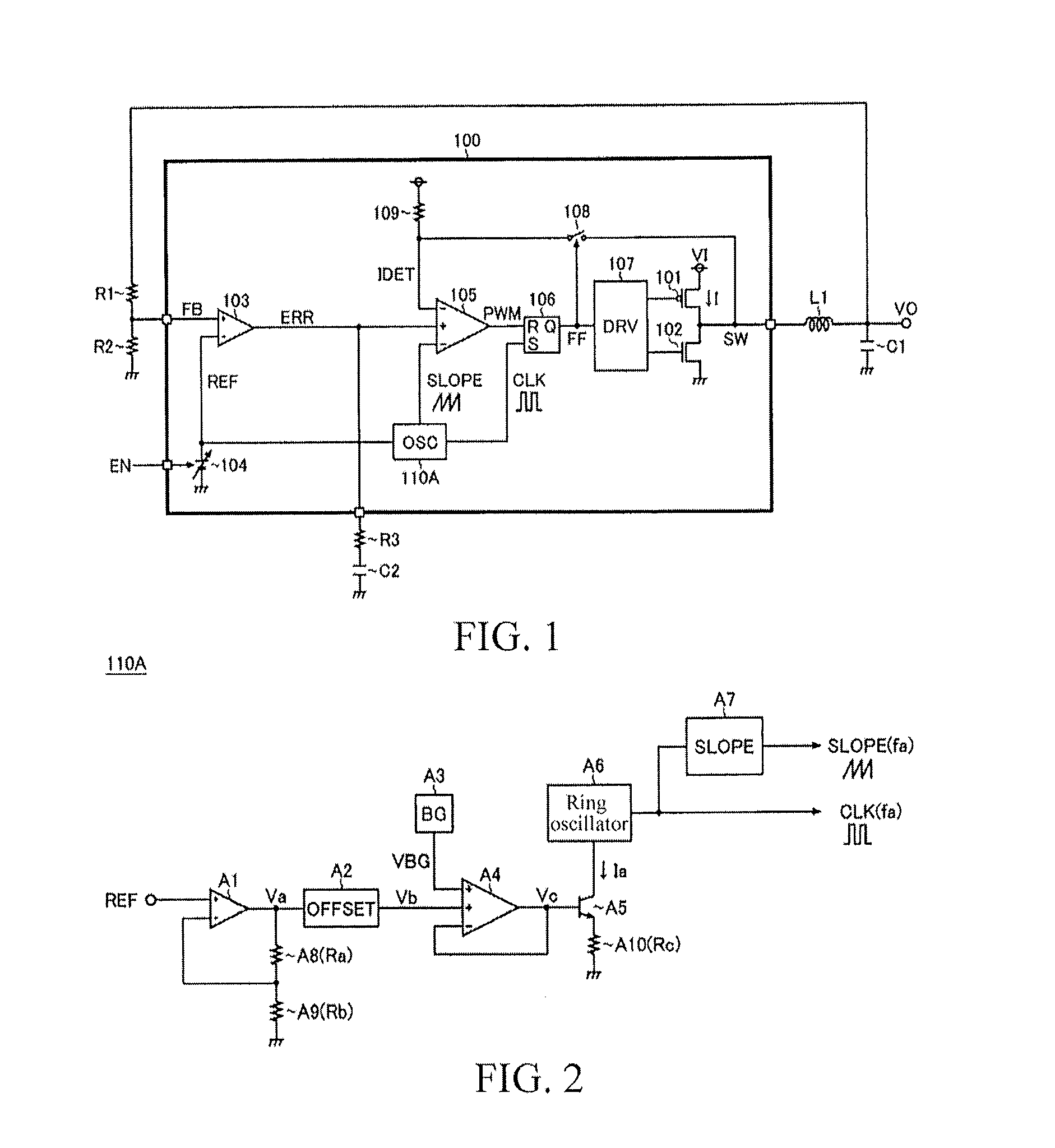
[0061]FIG. 1 is a block diagram of a current mode synchronous rectification DC / DC converter according to a first embodiment of the present invention. The current mode synchronous rectification DC / DC converter in the embodiment is formed by using a semiconductor device 100 (a so-called switching power supply integrated circuit (IC)), an inductor L1 hung externally thereon, capacitors C1 and C2, and resistors R1-R3, so an input voltage V1 is reduced to generate a required output voltage VO.

[0062]In the semiconductor device 100, an output transistor 101, a synchronous rectification transistor 102, an error amplifier 103, a reference voltage generation unit 104, a PWM comparator 105, an RS trigger 106, a driver 107, a switch 108, a pull up resistor 109, and an oscillator 110A are integrated. In addition, in the semiconductor device 100, in addition to the circuit elements, other protection circuits (such as a low input faulty action prevention circuit or a temperature protection circuit...

second embodiment

[0099]FIG. 4 is a block diagram of a current mode synchronous rectification DC / DC converter according to a second embodiment. The basic structure of the second embodiment is the same as that of the first embodiment same, so for circuit elements the same as those in the first embodiment, the same symbols as those in FIG. 1 are marked and repeated illustration is omitted. The circuit elements special to the second embodiment are illustrated explicitly below.

[0100]First, the current mode synchronous rectification DC / DC converter in the second embodiment has a frequency fixed type oscillator 110B to replace the frequency variable type oscillator 110A. The oscillator 110B has the circuit structure obtained by removing the operational amplifier A1, the offset setting unit A2, and the resistors A8 and A9 among the circuit elements that form the oscillator 110A in FIG. 2.

[0101]Also, the current mode synchronous rectification DC / DC converter in the second embodiment has a mask circuit (a com...

third embodiment

[0109]FIG. 6 is a block diagram of a current mode synchronous rectification DC / DC converter according to a third embodiment. The third embodiment has a stricture combining the first embodiment and the second embodiment. That is, the current mode synchronous rectification DC / DC converter in the third embodiment includes a frequency variable type oscillator 110A in FIG. 1 and includes a mask circuit (a comparator 111, a threshold voltage generation unit 112, and an N-channel type MOS field effect transistor 113) in FIG. 4.

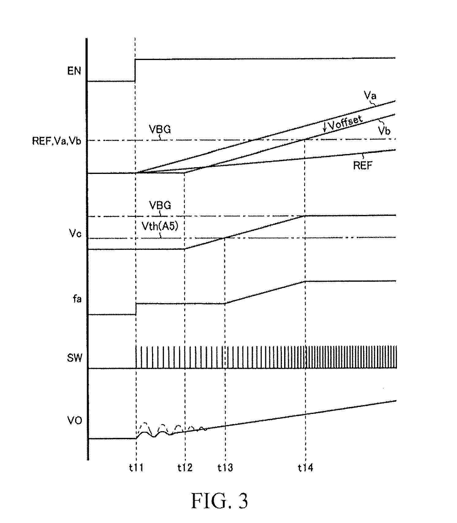
[0110]FIG. 3 is a sequence diagram of a start waveform according to a third embodiment. Starting from the top, the actions of an enable signal EN, a reference voltage REF, a first voltage Va, a second voltage Vb, a third voltage Vc, an oscillation frequency fa, a mask signal MSK, a switch voltage SW, and an output voltage VO are illustratively represented in sequence.

[0111]At time t31, if the enable signal EN is transitioned to a high level (a logic level when the ac...


PUM


Abstract

A current mode synchronous rectification direct current (DC)/DC converter according to the present invention includes: a soft start function unit (in FIG. 1, a reference voltage generation unit (104) enabling a reference voltage REF to slowly increase while starting), for inhibiting a target value of an output voltage VO to be lower than that at a normal action while starting; and an output stabilization function unit (in FIG. 1, a frequency variable type oscillator (110A) generating a clock signal CLK and a slope voltage SLOPE through an oscillation frequency corresponding to a reference voltage REF), for performing at least one of waiting for start of a switching action and reduction of a drive frequency while starting.

Description

BACKGROUND OF THE INVENTION[0001]1. Field of the Invention[0002]The present invention relates to a current mode synchronous rectification DC / DC converter that generates a required output voltage from an input voltage.[0003]2. Description of the Related Art[0004]The switching type DC / DC converter (also known as switching regulator) has been widely used for a long time as a reasonably efficient regulated power supply with limited thermal loss in applications where there is a clear, substantial difference between input and output. Such a device operates by driving an energy storage element (a capacitor or an inductor) through turn-on / turn-off control (power (duty) control) of an output transistor, so as to generate a required output voltage from an input voltage.[0005]In addition, for a switching type DC / DC converter requiring a high conversion efficiency, a synchronous rectification manner is commonly adopted to greatly reduce a turn-on resistance of a rectification element; that is, ...

Claims


Application Information

Patent Timeline
Patent Type & Authority Applications(United States)
IPC IPC(8): G05F1/46
CPCH02M1/36Y02B70/1466H02M3/1588Y02B70/10
Inventor YAMAKOSHI, HARUONAKABAYASHI, HIROTAKA
Owner ROHM CO LTD
Why Eureka
Try Eureka