Circuit and system of a high density Anti-fuse

a high-density anti-fuse, circuit technology, applied in the direction of instruments, basic electric elements, semiconductor devices, etc., can solve the problems of high manufacturing cost, high breakdown voltage, difficult manufacturing, etc., and achieve the effect of high fabrication cos

Active Publication Date: 2012-06-14
ATTOPSEMI TECH CO LTD
View PDF8 Cites 105 Cited by
  • Summary
  • Abstract
  • Description
  • Claims
  • Application Information

AI Technical Summary

Benefits of technology

[0008]Another key concept of this invention is to use core logic or I / O devices in the peripheral of the anti-fuse memory that are the same devices as those built in the rest of integrated circuits. In the past, the programming voltage of an anti-fuse is very high, about 12V or 18V, that needs special high voltage devices in the peripheral circuit to design an anti-fuse memory. As a result, more mask layers and more process steps are needed, and hence the fabrication costs are very high. One aspect of this invention can eliminate the need to use high voltage devices to lower the breakdown voltage of the dielectric film so that core or I / O devices in an integrated circuit can be used. Another embodiment is to use a combination of different voltages in two perpendicular conductors to achieve high voltage for a selected cell to program, while the unselected cells are operated within a low voltage range.

Problems solved by technology

Alternatively other types of metal oxides, such as Al2O3, HfO2, MgO, ZrO2, or Cr2O3, can be used, but they may be more expensive, difficult to manufacture, and have a higher breakdown voltage.
As a result, more mask layers and more process steps are needed, and hence the fabrication costs are very high.

Method used


Image

  • Circuit and system of a high density Anti-fuse
  • Circuit and system of a high density Anti-fuse
  • Circuit and system of a high density Anti-fuse

Examples


Embodiment Construction

[0056]This invention concerns a dielectric breakdown anti-fuse cell using diode as program selector defined at a cross-point of two conductor lines in perpendicular directions. Various embodiments about dielectric materials, diode structures, conductor types, process steps, devices employed, and cell select schemes will be disclosed and that are within the scope of this invention.

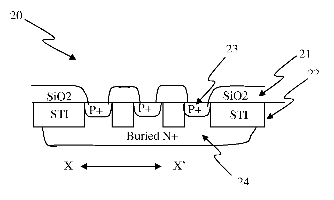
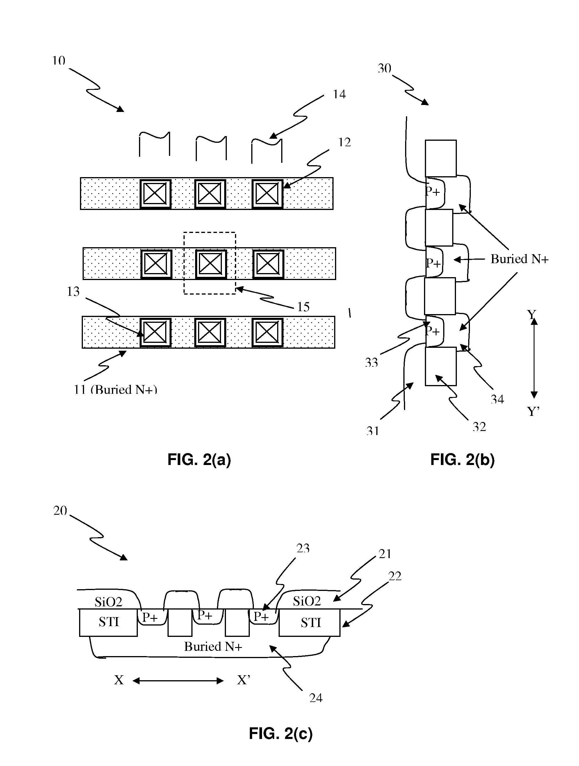
[0057]FIG. 2(a) shows a top view of a dielectric breakdown anti-fuse 10 according to one embodiment. Each anti-fuse cell 15 is defined by active regions in X- and Y-directions. An array of buried N+ lines 11 serve as wordlines are built running in the X-direction before active regions 12 is defined. The active regions can be isolated in X- and Y-directions by Local Oxidation (LOCOS) or Shallow Trench Isolation (STI). A contact hole 13 in each active region is etched after depositing an interlayer dielectric. Then, N type and P type dopants are subsequently implanted into the contact hole in each active regi...


PUM


Abstract

A high density anti-fuse cell can be built at the cross points of two perpendicular interconnect lines, such as active region lines, active and polysilicon lines, active and metal lines, or polysilicon and metal lines. The cell size can be very small. At least one of the anti-fuse cells have a thin oxide fabricated before, after, or between a diode in at least one contact holes at the cross points of the interconnect lines. The thin oxide of the anti-fuse cells at the cross points can be selected for rupture by applying supply voltages in the two perpendicular lines. In some embodiments, a diode can be created after thin oxide is ruptured so that explicitly fabricating a diode or opening a contact hole at the cross-point may not be necessary.

Description

CROSS-REFERENCE TO RELATED APPLICATION[0001]This application claimed priority benefit of U.S. Provisional Patent Application No. 61 / 421,184 filed on Dec. 8, 2010, titled “Method and Apparatus of A High Density Anti-fuse,” which is hereby incorporated herein by reference.BACKGROUND OF THE INVENTION[0002]Anti-fuse is one of the One-Time Programmable (OTP) devices that can only be programmed once. Particularly, an anti-fuse has a high impedance state after fabrication and a low impedance state after being programmed. On the contrary, a fuse has a low impedance state after fabrication and a high impedance state after being programmed. The most commonly used anti-fuses are based on MOS gate oxide breakdown, metal-dielectric-metal breakdown, metal-dielectric-silicon breakdown, or silicon-dielectric-silicon breakdown, etc. Silicon dioxide (SiO2) is the most commonly used dielectric for breakdown in anti-fuses. However, Silicon-Oxide-Nitride (SON), Silicon Nitride (SiNx), Oxide-Nitride-Oxid...

Claims


Application Information

Patent Timeline
Patent Type & Authority Applications(United States)
IPC IPC(8): G11C17/08
CPCH01L23/5252H01L27/101G11C17/16H01L2924/0002H01L2924/00
Inventor CHUNG, SHINE C.
Owner ATTOPSEMI TECH CO LTD
Why Eureka
Try Eureka