Photovoltaic devices with an interfacial germanium-containing layer and methods for forming the same

a photovoltaic device and germanium-containing technology, applied in the field of photovoltaic devices, can solve problems such as the heat of irradiated materials, achieve the effects of increasing the fill factor and the efficiency reducing the series resistance, and increasing the shunt resistance of the photovoltaic devi

Inactive Publication Date: 2012-06-21
IBM CORP +1
View PDF6 Cites 18 Cited by
  • Summary
  • Abstract
  • Description
  • Claims
  • Application Information

AI Technical Summary

Benefits of technology

[0007]A germanium-containing layer is provided between a p-doped silicon-containing layer and a transparent conductive material layer of a photovoltaic device. The germanium-containing layer can be a silicon-germanium alloy layer or a germanium layer. The germanium-containing layer has a greater atomic concentration of germanium than the p-doped silicon-containing layer. The presence of the germanium-containing layer has the effect of reducing the series resistance and increasing the shunt resistance of the photovoltaic device, thereby increasing the fill factor and the efficiency of the photovoltaic device.

Problems solved by technology

Thus, in the absence of any electrical bias, photogeneration of electron-hole pairs merely results in heating of the irradiated material.

Method used


Image

  • Photovoltaic devices with an interfacial germanium-containing layer and methods for forming the same
  • Photovoltaic devices with an interfacial germanium-containing layer and methods for forming the same
  • Photovoltaic devices with an interfacial germanium-containing layer and methods for forming the same

Examples


Embodiment Construction

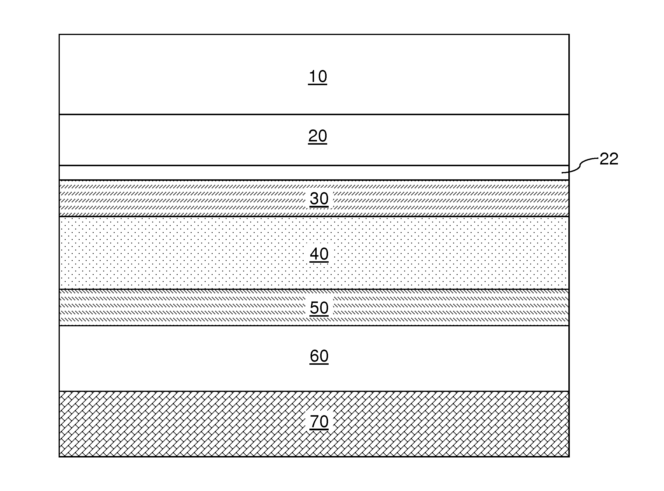
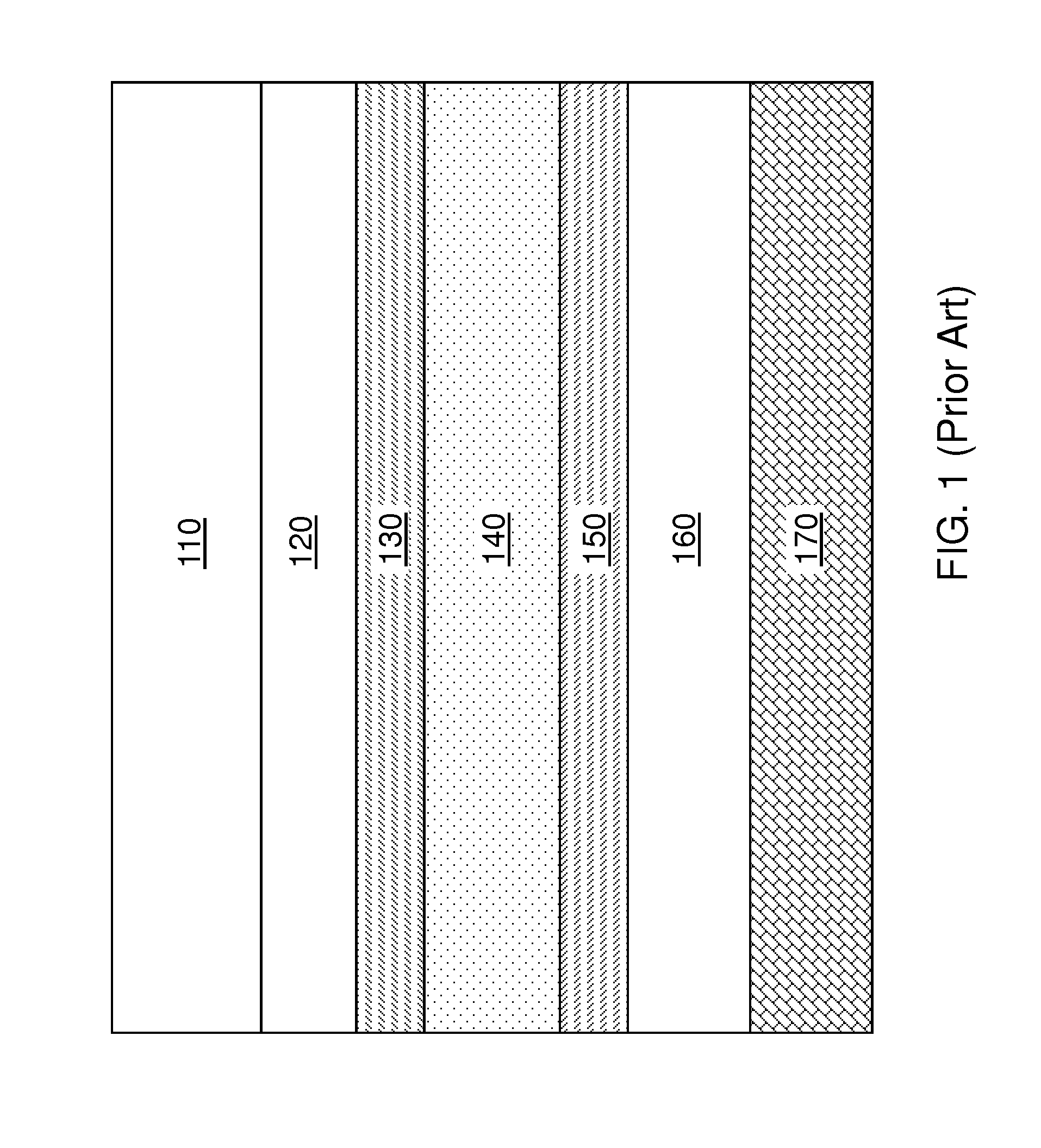
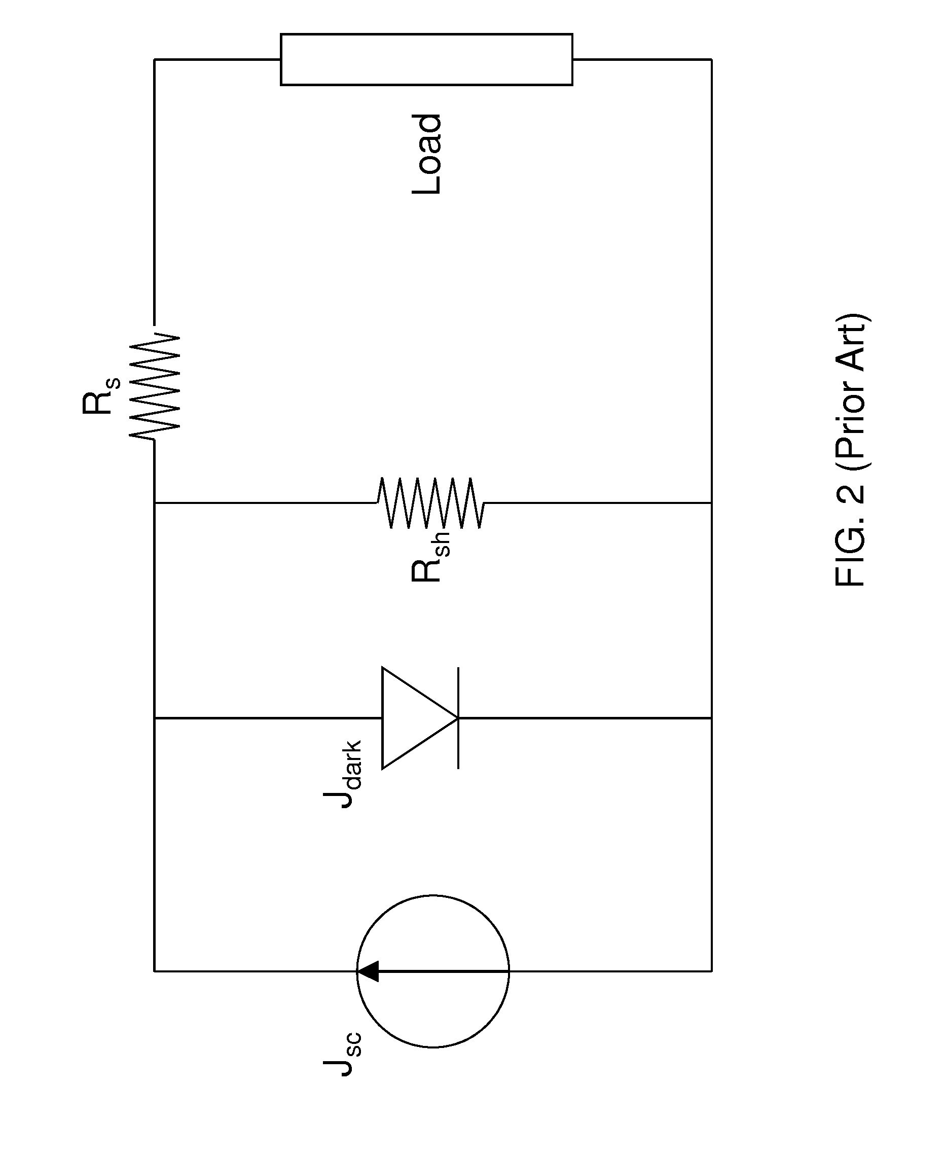
[0020]As stated above, the present disclosure relates to photovoltaic devices including an interfacial germanium-containing layer and methods of forming the same, which are now described in detail with accompanying figures. Throughout the drawings, the same reference numerals or letters are used to designate like or equivalent elements. The drawings are not necessarily drawn to scale.

[0021]As used herein, a crystal structure is “microcrystalline” if the average grain size of the material is from 1 nm to 10 microns.

[0022]As used herein, a “hydrogenated” semiconductor material is a semiconductor material including incorporated hydrogen therein, which neutralizes dangling bonds in the semiconductor material and allows charge carriers to flow more freely.

[0023]As used herein, a “semiconductor-material-containing reactant gas” refers to a gas including at least one atom of Si, Ge, or components of a compound semiconductor material.

[0024]As used herein, an element is “optically transparen...


PUM

PropertyMeasurementUnit
grain sizeaaaaaaaaaa
Fermi level EFaaaaaaaaaa
work functionaaaaaaaaaa

Abstract

A germanium-containing layer is provided between a p-doped silicon-containing layer and a transparent conductive material layer of a photovoltaic device. The germanium-containing layer can be a p-doped silicon-germanium alloy layer or a germanium layer. The germanium-containing layer has a greater atomic concentration of germanium than the p-doped silicon-containing layer. The presence of the germanium-containing layer has the effect of reducing the series resistance and increasing the shunt resistance of the photovoltaic device, thereby increasing the fill factor and the efficiency of the photovoltaic device. In case a silicon-germanium alloy layer is employed, the closed circuit current density also increases.

Description

BACKGROUND[0001]The present disclosure relates to photovoltaic devices, and more particularly to photovoltaic devices including an interfacial germanium-containing layer and methods of forming the same.[0002]A photovoltaic device is a device that converts the energy of incident photons to electromotive force (e.m.f.). Typical photovoltaic devices include solar cells, which are configured to convert the energy in the electromagnetic radiation from the Sun to electric energy. Each photon has an energy given by the formula E=hν, in which the energy E is equal to the product of the Plank constant h and the frequency ν of the electromagnetic radiation associated with the photon.[0003]A photon having energy greater than the electron binding energy of a matter can interact with the matter and free an electron from the matter. While the probability of interaction of each photon with each atom is probabilistic, a structure can be built with a sufficient thickness to cause interaction of phot...

Claims


Application Information

Patent Timeline
Patent Type & Authority Applications(United States)
IPC IPC(8): H01L31/0264H01L31/18
CPCH01L31/02167Y02E10/548H01L31/1816H01L31/075
Inventor CHEN, TZE-CHIANGKIM, JEE H.SADANA, DEVENDRA K.ABOU-KANDIL, AHMEDSAAD, MOHAMED
Owner IBM CORP
Why Eureka
Try Eureka