Oscillator, and clock generator, semiconductor device, and electronic device including the same
a clock generator and oscillator technology, applied in oscillator generators, pulse automatic control, instruments, etc., can solve the problems of deterioration of oscillator jitter characteristics, adversely affecting the oscillator oscillation property, extraneous power consumption, etc., to prevent deterioration of oscillation property and reduce extraneous power consumption and noise occurren
- Summary
- Abstract
- Description
- Claims
- Application Information
AI Technical Summary
Benefits of technology
Problems solved by technology
Method used
Image
Examples
first embodiment
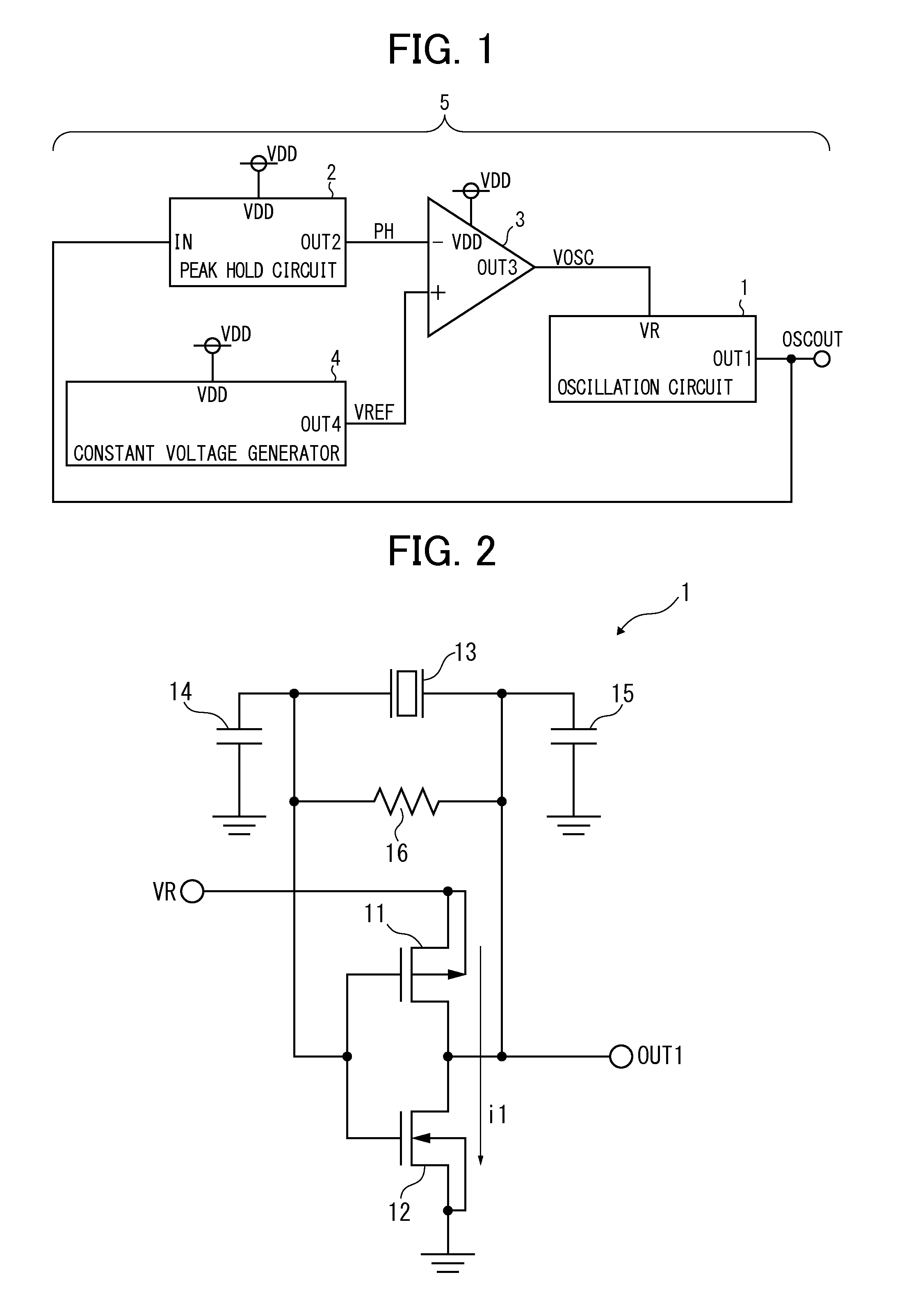
[0039]FIG. 1 shows the structure of an oscillator according to a first embodiment of the present invention by way of example.
[0040]In FIG. 1 an oscillator 5 is used in a real-time clock system having a timer or calendar function, a clock generator circuit to generate system clock signals for a microprocessor or else, or a reference clock generator circuit for a communication device. It includes an oscillation circuit 1 as an oscillation element, a peak hold circuit 2, a regulator 3 as a controller, and a constant voltage generator 4 as a reference voltage generator.
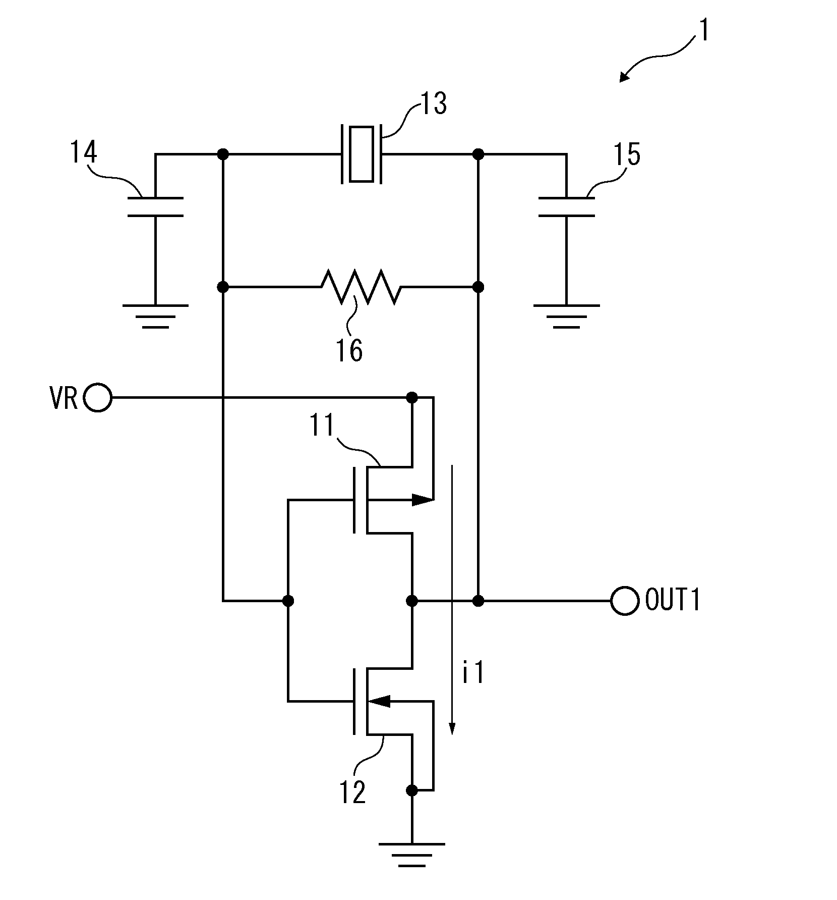
[0041]The oscillation circuit 1 uses a crystal oscillator element or the like to output an oscillation signal OSCOUT from an output terminal OUT1. The oscillation signal OSCOUT is used in a clock system or the like and input to an input terminal IN of the peak hold circuit 2.
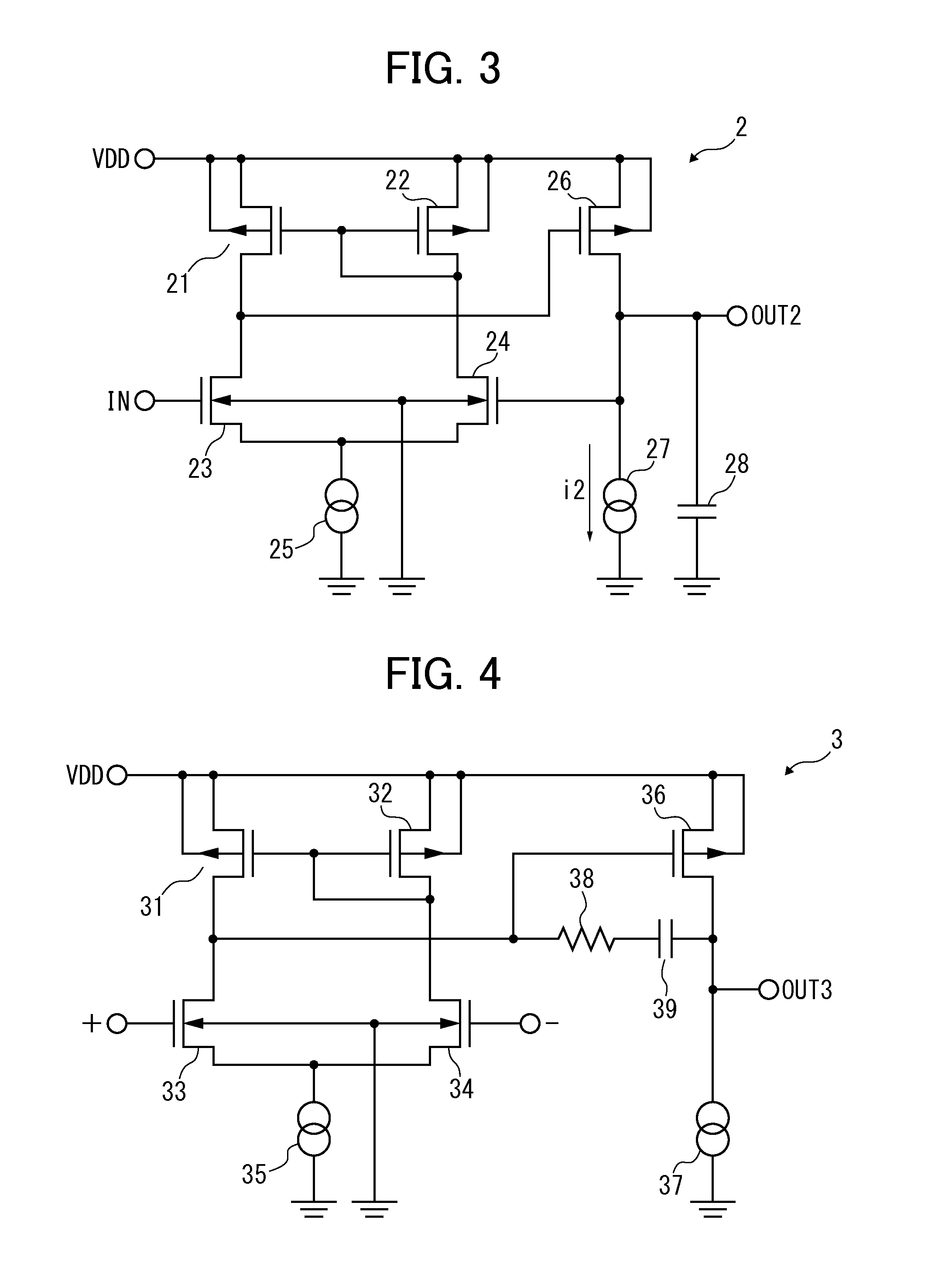
[0042]The peak hold circuit 2 holds a voltage with a maximal value or peak of the amplitude of the oscillation signal OSCOUT for a certain period of ...
second embodiment
[0114]In the second embodiment an oscillator including a bottom hold circuit in replace of the peak hold circuit is described with reference to FIG. 7A. The oscillator in the second embodiment can attain the same effects as those in the first embodiment. The reference voltage VREF is set to around a GND voltage (0V).
[0115]An oscillator 5a in FIG. 7A includes an oscillation circuit 51, a bottom hold circuit 52, a regulator 53 and a constant voltage generator 54.
[0116]The bottom hold circuit 52 holds a bottom value of the oscillation signal OSCOUT from the oscillation circuit 51 as a bottom hold voltage BH and outputs the voltage BH to a positive input of the regulator 53 and the reference voltage VREF to a negative input thereof. The regulator 53 controls the drive voltage VOSC of the oscillation circuit 51 so that the bottom hold voltage BH coincides with the reference voltage VREF.
[0117]The oscillation circuit 1 uses a crystal oscillator element or the like to output the oscillatio...
PUM
 Abstract
Description
Claims
Application Information


