Solid-state imaging device, process of making solid state imaging device, digital still camera, digital video camera, mobile phone, and endoscope

a solid-state imaging and imaging device technology, applied in the field of solid-state imaging devices, can solve the problems of reducing the effective area of the photodiode, reducing the aperture ratio, and reducing the pixel aperture ratio, so as to prevent color cross-talk between pixels and lower refractive index.

Active Publication Date: 2012-06-28
FUJIFILM CORP
View PDF6 Cites 47 Cited by
  • Summary
  • Abstract
  • Description
  • Claims
  • Application Information

AI Technical Summary

Benefits of technology

[0214]If desired, the colored thermosetting composition may contain various additives as long as such does not affect the effects of the invention. Examples of additives include binders, curing agents, curing catalysts, solvents, fillers, polymeric compounds other than those described, surfactants, adhesion enhancer, antioxidants, UV absorbers, anti-coagulants, and dispersants.
[0215]In the cases where color filters of different colors are formed by dry etching, an etching resist pattern is formed using a photoresist as described. In the step of removal, too, a resist pattern is preferably formed using a photoresist.
[0216]The positively working photosensitive resin composition as a positive photoresist may be a positive photoresist composition sensitive to a radiation, such as UV radiation (g-line, h-line, or i-line of mercury lamps), deep UV radiation (including an excimer laser beam), an electron beam, an ion beam, and X-rays. Of the radiations described, preferred are g-line, h-line, and i-line. An i-line is particularly preferred.
[0217]Specifically, the positive photosensitive resin composition preferably contains a quinonediazide compound and an alkali soluble resin. On being irradiated with a radiation of 500 nm or shorter wavelengths, the quinonediazide group of the quinonediazide compound decomposes to produce a carboxyl group, whereby the alkali insoluble composition turns to alkali soluble. The positive photoresist of this type has remarkably high resolution and is widely used in the semiconductor fabrication. The quinonediazide compound is exemplified by a naphthoquinonediazide compound.
[0218]Any developer may be used as long as it is capable of dissolving the exposed area of a positive photoresist or the unexposed area of a negative photoresist without affecting the peripheral light shielding layer. Specifically, a combination of various solvents or an aqueous alkali solution may be used.
[0219]While the steps of forming color filters of different colors have been described with particular reference to color filters of primary color (RBG) system, these steps are also applicable to the formation of color filters of complementary color system using cyan, magenta, yellow, and green.

Problems solved by technology

Therefore, as the pixel pitch reduces, the area ratio of the circuit region in unit pixel becomes larger, which of necessity raises the problem of reduction in the effective area of the photodiode, i.e., reduction of a pixel aperture ratio.
Reduction of aperture ratio leads to reduction of sensitivity.

Method used


Image

  • Solid-state imaging device, process of making solid state imaging device, digital still camera, digital video camera, mobile phone, and endoscope
  • Solid-state imaging device, process of making solid state imaging device, digital still camera, digital video camera, mobile phone, and endoscope
  • Solid-state imaging device, process of making solid state imaging device, digital still camera, digital video camera, mobile phone, and endoscope

Examples


example 1

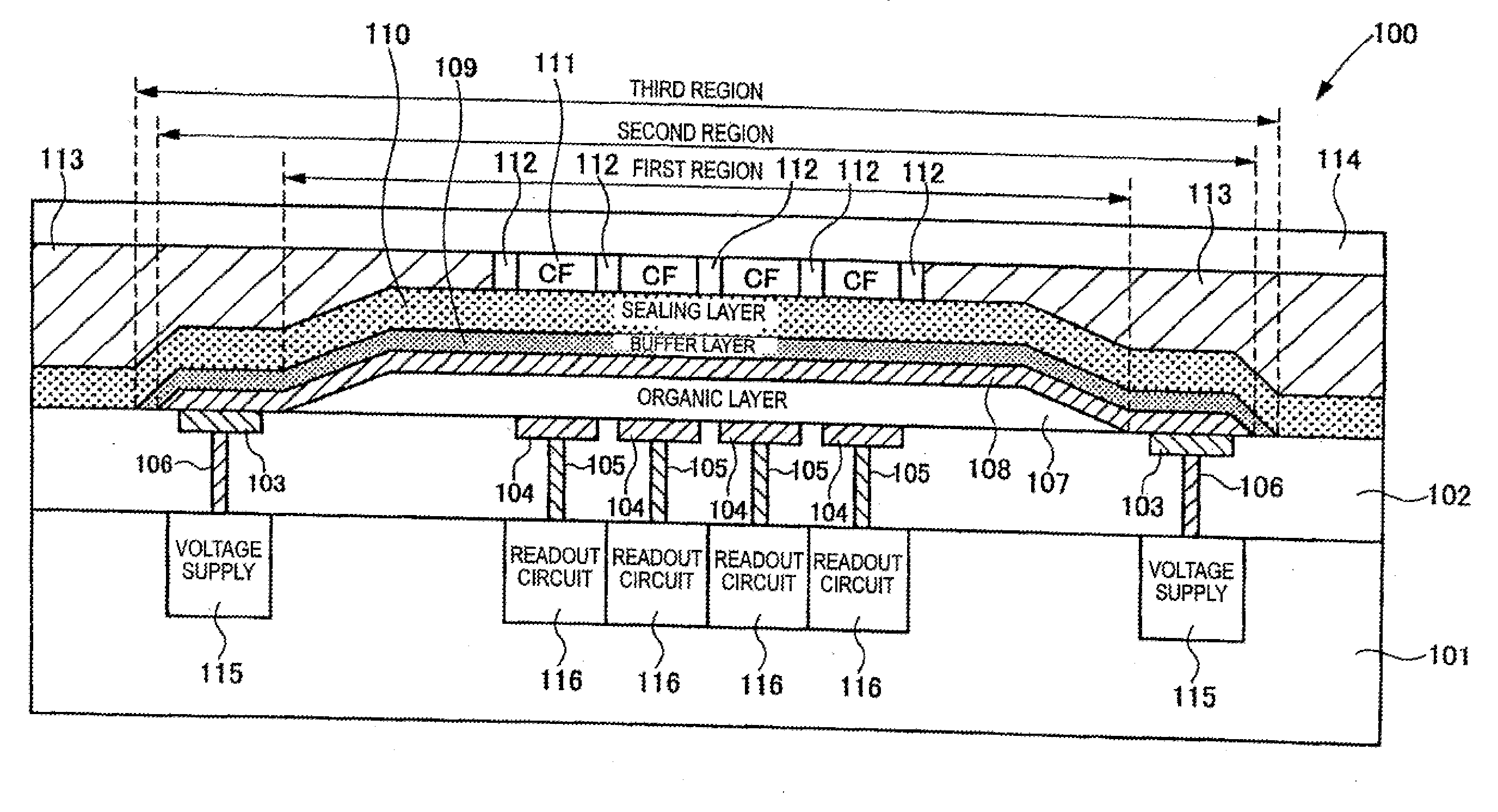
[0271]A solid state imaging device having the structure of FIG. 53 was fabricated. Both the pixel electrodes 104 and the via plugs 105 were made of tungsten by the dual damascene process described supra. Specifically, TiN was sputtered as a barrier metal, followed by formation of a tungsten film by CVD, and the surface was planarized by CMP. The pixel electrodes 104 had a thickness of 300 nm and a generally square shape with a length and a width of 1.4 μm.

example 2

[0272]A solid state imaging device was fabricated in the same manner as in Example 1, except that the pixel electrodes 104 and the via plugs 105 were formed by first depositing a stack of tantalum nitride as barrier metal and copper by sputtering and then depositing a copper layer by plating, followed by planarization by CMP.

[0273]The results of characterization of the solid state imaging devices fabricated in Examples 1 and 2 are summarized in Table 1. The characteristics as referred to in these and other Examples were determined as follows.

(1) Level Difference A

[0274]The level difference A between the surface of the pikel electrode 104 and the surface of the dielectric layer between adjacent pixel electrodes 104 was obtained by observing a cross-section of the device under an electron microscope.

(2) Δ1 and Δ2

[0275]The difference Δ1 between the electron affinity Ea of the organic n type semiconductor (C60) and the ionization potential Ip of the charge blocking layer 15a and the dif...

example 3

[0278]Solid state imaging devices having a varied level difference A were fabricated in the same manner as in Example 1, except that the pixel electrodes 104 were formed by the above described trench isolation technique. Specifically, a TiN (thickness: 30 nm) was deposited by CVD on the dielectric layer 102 and the via plugs 105 previously formed by the standard CMOS image sensor processes. The TiN layer was patterned by the CMOS image sensor processes to leave arrays of generally square shaped TiN layer with a length and a width of 1.4 μm. The same dielectric material as the dielectric layer 102 was deposited on the dielectric layer 102 and the TiN layer. Finally, the deposited dielectric layer was planarized, by CMP until the top surface of the TiN layer (pixel electrodes 104) was exposed. The time of CMP was varied to result in different level difference A among the devices.


PUM


Abstract

A solid-state imaging device includes a substrate, a dielectric layer on the substrate, and an array of pixels, each of the pixels includes: a pixel electrode, an organic layer, a counter electrode, a sealing layer, a color filter, a readout circuit and a light-collecting unit as defined herein, the photoelectric layer contains an organic p-type semiconductor and an organic n-type semiconductor, the organic layer further includes a charge blocking layer as defined herein, an ionization potential of the charge blocking layer and an electron affinity of the organic n-type semiconductor present in the photoelectric layer have a difference of at least 1 eV, and a surface of the pixel electrodes on a side of the photoelectric layer and a surface of the dielectric layer on a side of the photoelectric layer are substantially coplanar.

Description

TECHNICAL FIELD[0001]This invention relates to a solid-state imaging device, a method of making a solid state imaging device, a digital still camera, a digital video camera, a mobile phone, and an endoscope.BACKGROUND ART[0002]As image sensors mounted on digital still cameras, digital video cameras, mobile phone cameras, and endoscope cameras, solid state imaging apparatus called CCD sensors or CMOS sensors which include a substrate, e.g., a silicon chip, and an array of pixels containing a photodiode and read out signal charge corresponding to photoelectrons generated in the photodiode of each pixel by a CCD or CMOS readout circuit are known.[0003]The known solid state imaging apparatus includes not only the photodiode but a signal readout circuit and an accompanying multilevel interconnect formed on the semiconductor substrate for every pixel. Therefore, as the pixel pitch reduces, the area ratio of the circuit region in unit pixel becomes larger, which of necessity raises the pro...

Claims


Application Information

Patent Timeline
Patent Type & Authority Applications(United States)
IPC IPC(8): H01L31/0232H01L31/18
CPCB82Y10/00H01L27/307H01L51/4253H01L51/0047H01L51/0059H01L51/001H10K39/32H10K71/164H10K85/215H10K85/631H10K30/30H01L27/146H04N25/00
Inventor MAEHARA, YOSHIKIGOTO, TAKASHISUZUKI, HIDEYUKI
Owner FUJIFILM CORP
Why Eureka
Try Eureka