Three-dimensional system-in-package package-on-package structure

a three-dimensional system and package technology, applied in the field of package structure, can solve the problems of time-consuming manufacturing process, inability to meet the demand of producing a smaller chip with high density elements on the chip, and complicated semiconductor devices

Active Publication Date: 2012-06-28
ADL ENERGY CORP
View PDF1 Cites 55 Cited by
  • Summary
  • Abstract
  • Description
  • Claims
  • Application Information

AI Technical Summary

Benefits of technology

[0006]Though WLP technique has the advantages mentioned above, some issues still exist influencing the acceptance of WLP technique. For example, although utilizing WLP technique can reduce the CTE mismatch between IC and the interconnecting substrate, as the size of the device minimizes, the CTE difference between the materials of a structure of WLP becomes another critical factor to mechanical instability of the structure. Furthermore, in this wafer-level chip-scale package, a plurality of bond pads formed on the semiconductor die is redistributed through conventional redistribution processes involving a redistribution layer into a plurality of metal pads in an area array type. Solder balls are directly fused on the metal pads, which are formed in the area array type by means of the redistribution process. Typically, all of the stacked redistribution layers are formed over the built-up layer over the die. Therefore, the thickness of the package is increased. This may conflict with the demand of reducing the size of a chip.

Problems solved by technology

As semiconductors become more complicated, the traditional package techniques, for example lead frame package, flex package, and rigid package technique, cannot meet the demand of producing a smaller chip with high density elements on the chip.
Therefore, these techniques are time consuming for the manufacturing process.
Therefore, as the size of electronics has become demanding, so does the package technique.
Though WLP technique has the advantages mentioned above, some issues still exist influencing the acceptance of WLP technique.
For example, although utilizing WLP technique can reduce the CTE mismatch between IC and the interconnecting substrate, as the size of the device minimizes, the CTE difference between the materials of a structure of WLP becomes another critical factor to mechanical instability of the structure.
This may conflict with the demand of reducing the size of a chip.
Unfortunately, leadframe based three-dimensional packages have lagged in their ability to handle the increase in circuit density required of high level functionally integrated systems.
Typically, leadframe packaging has its limit due to factors such as, increased package thickness, a larger footprint area, and insufficient input / output leads to handle the higher circuit density.

Method used


Image

  • Three-dimensional system-in-package package-on-package structure
  • Three-dimensional system-in-package package-on-package structure
  • Three-dimensional system-in-package package-on-package structure

Examples


Embodiment Construction

[0019]The invention will now be described in greater detail with reference to preferred embodiments of the invention and illustrations attached. Nevertheless, it should be recognized that the preferred embodiments of the invention are only for illustration. Besides the preferred embodiments mentioned here, the present invention can be practiced in a wide range of other embodiments besides those explicitly described, and the scope of the present invention is expressly not limited except as specified in the accompanying claims.

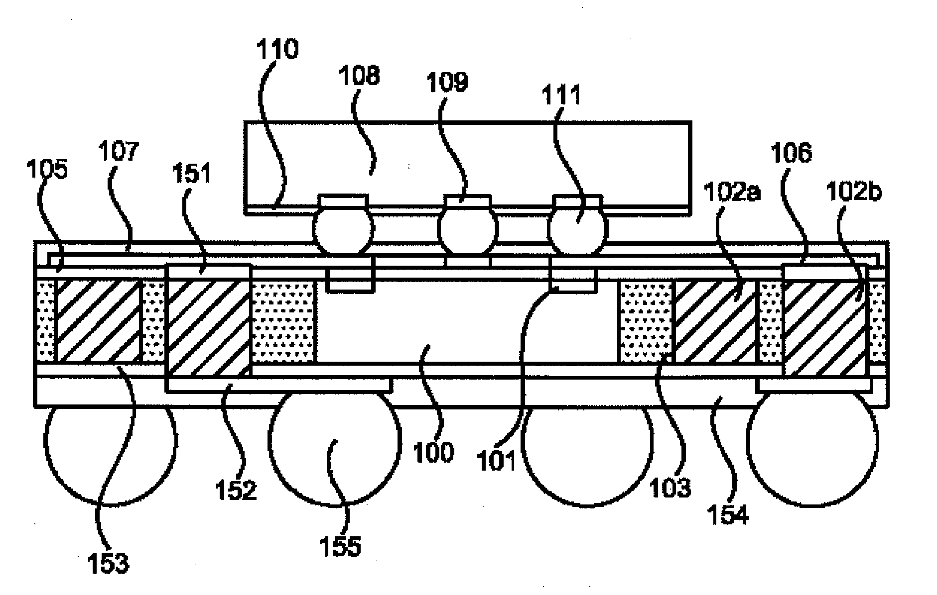
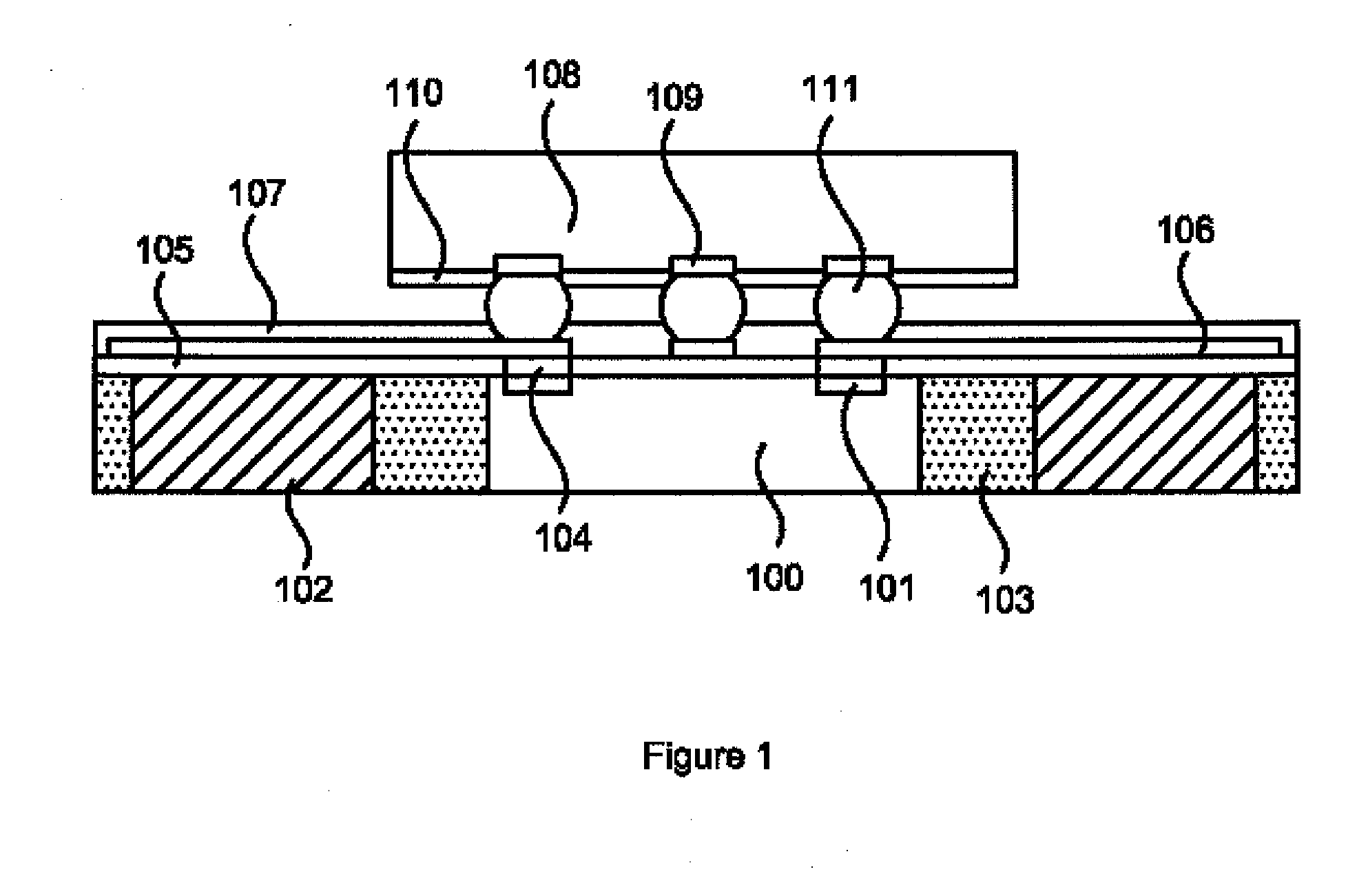
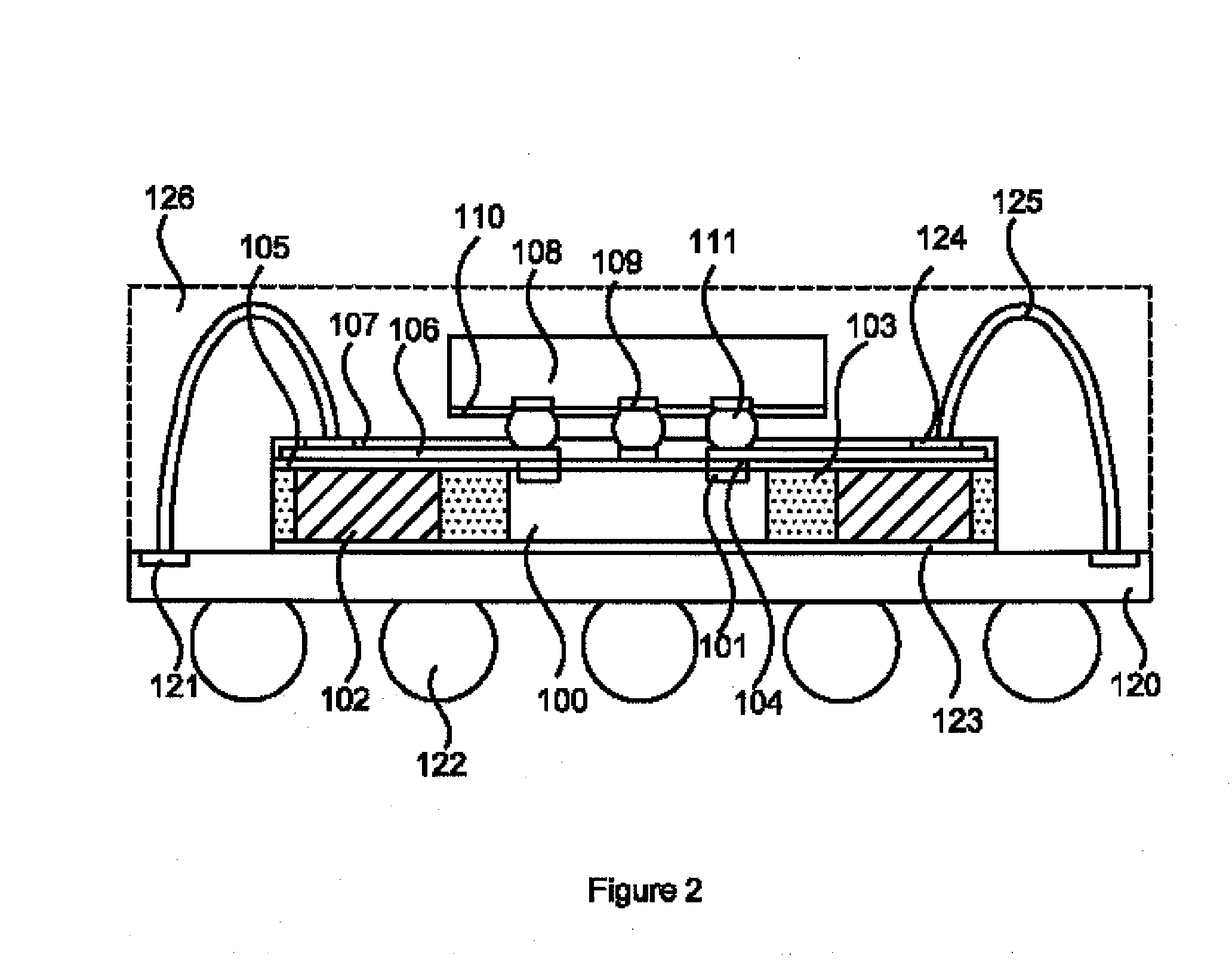
[0020]The present invention provides a newly three-dimensional System-In-Package (SiP) Package-On-Package (POP) structure for reducing the package thickness and area and for better board level reliability test of temperature cycling.

[0021]FIG. 1 illustrates a cross-sectional view of a basic three-dimensional System-In-Package (SiP) Package-On-Package (POP) structure in accordance with one embodiment of the present invention. As shown in the FIG. 1, the three-dim...


PUM


Abstract

The present invention provides a three-dimensional System-In-Package (SIP) Package-On-Package (POP) structure comprising a support element formed around a first electronic device. A filling material is filled between the first electronic device and the support element. Signal channels are coupled to first die pads of the first electronic device. Conductive elements form signal connection between the first end of the signal channels and the second die pads of a second electronic device.

Description

FIELD OF THE INVENTION[0001]This invention relates to a structure of package, and more particularly to a three-dimensional System-In-Package (SiP) Package-On-Package (POP) structure.DESCRIPTION OF THE PRIOR ART[0002]In the field of semiconductor devices, the device density is increased and the device dimension is reduced, continuously. The demand for the packaging or interconnecting techniques in such high density devices is also increased to fit the situation mentioned above. Conventionally, in the flip-chip attachment method, an array of solder bumps is formed on the surface of the die. The formation of the solder bumps may be carried out by using a solder composite material through a solder mask for producing a desired pattern of solder bumps. The function of chip package includes power distribution, signal distribution, heat dissipation, protection and support . . . and so on. As semiconductors become more complicated, the traditional package techniques, for example lead frame p...

Claims


Application Information

Patent Timeline
Patent Type & Authority Applications(United States)
IPC IPC(8): H01L23/498
CPCH01L23/49816H01L23/49827H01L23/5389H01L2224/48091H01L2924/09701H01L2224/73204H01L23/3128H01L24/48H01L2225/06527H01L23/562H01L24/05H01L24/13H01L24/14H01L24/16H01L24/19H01L24/20H01L24/29H01L24/32H01L24/73H01L24/96H01L2223/54433H01L2223/54486H01L2224/12105H01L2224/131H01L2224/1403H01L2224/29147H01L2224/2919H01L2225/0651H01L2224/02311H01L2225/06513H01L2224/05569H01L2224/0401H01L2224/04042H01L2224/04105H01L2224/05548H01L2224/16145H01L2224/32225H01L2224/48227H01L2224/73207H01L2224/73265H01L2924/15311H01L25/0657H01L2924/01029H01L2924/14H01L2924/15321H01L2924/19107H01L2924/10253H01L2924/3025H01L2924/00014H01L2924/00012H01L2924/014H01L2924/00H01L2224/05552H01L2224/73267H01L2924/18162H01L2924/351H01L2924/181H01L2224/16227H01L2224/45099H01L2224/45015H01L2924/207H01L2224/16225
Inventor LIN, NAN-CHUNCHENG, YA-YUN
Owner ADL ENERGY CORP
Why Eureka
Try Eureka