
Underfill for high density interconnect flip chips

Inactive Publication Date: 2012-07-05
NAMICS CORPORATION
View PDF6 Cites 23 Cited by
  • Summary
  • Abstract
  • Description
  • Claims
  • Application Information

AI Technical Summary

Benefits of technology

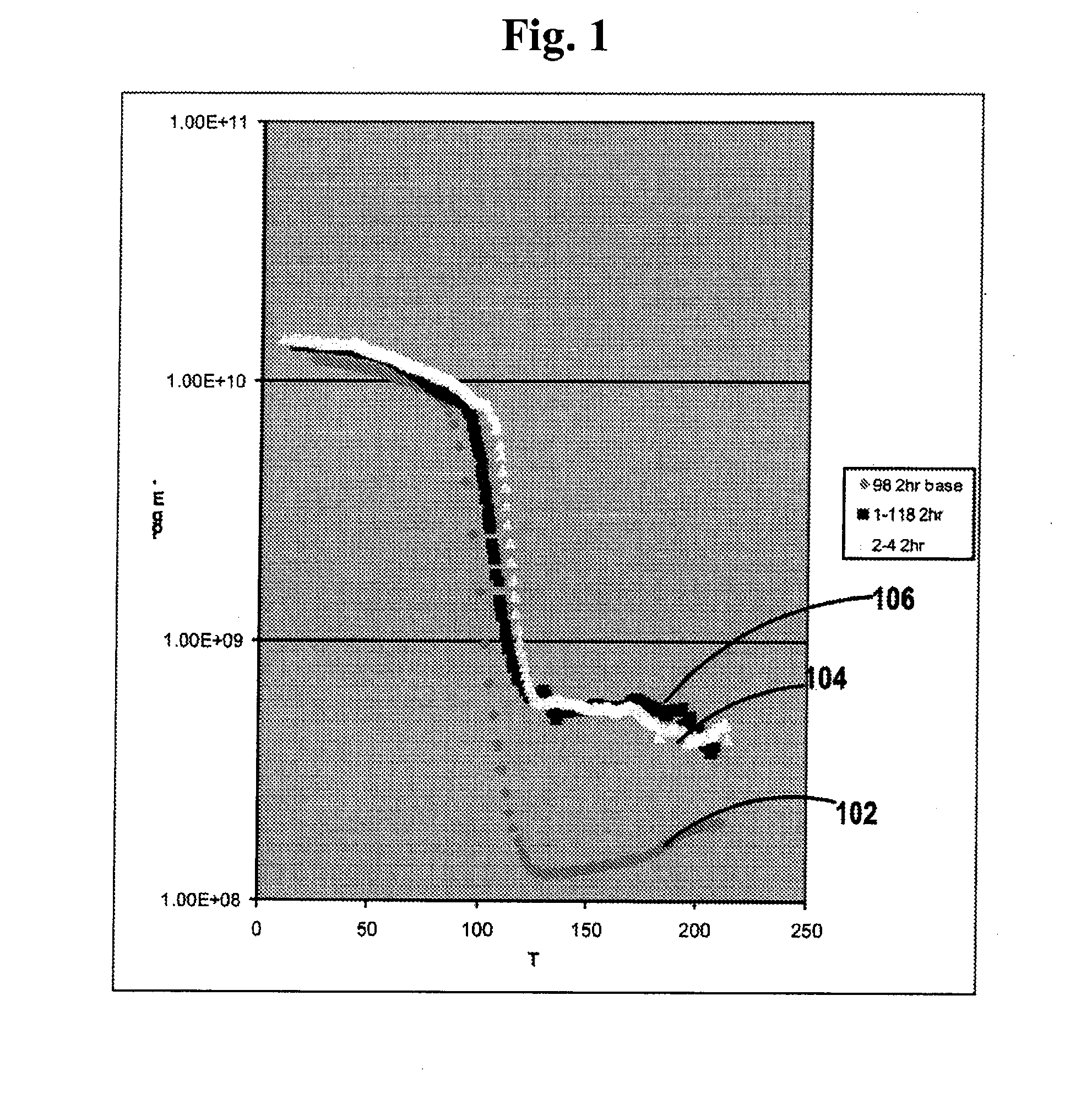
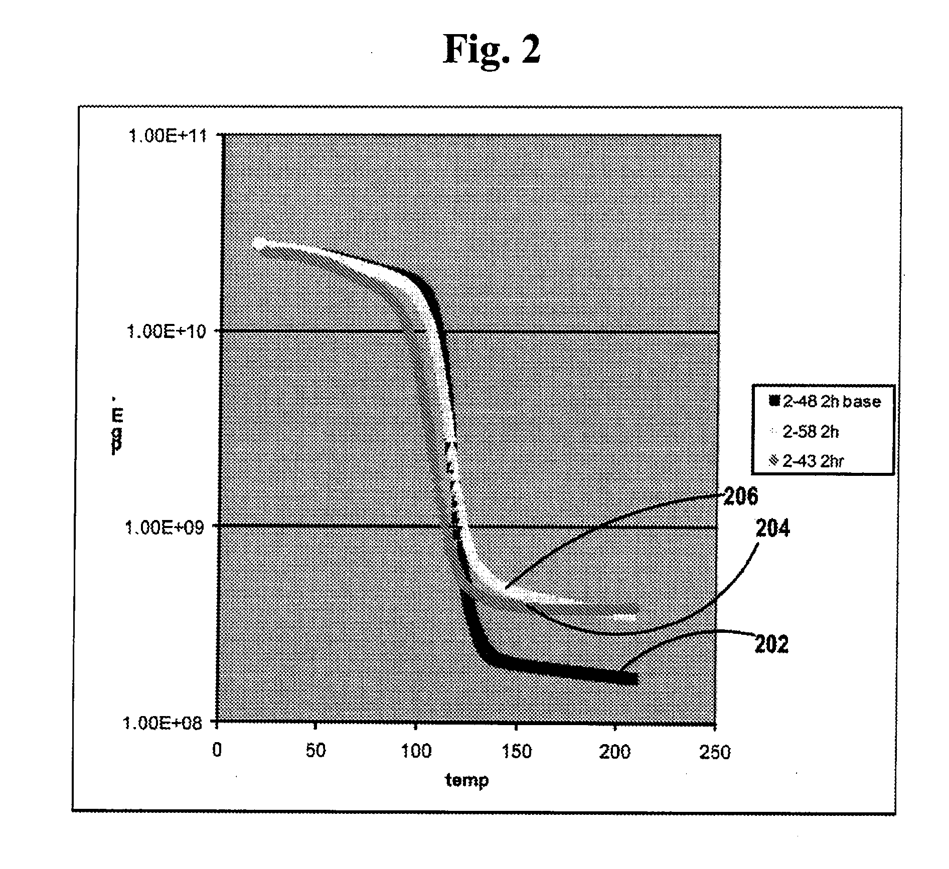
[0011]Certain embodiments of the invention provide additives to an underfill base formulation wherein the additives provides enhanced properties. In certain embodiments the base formulation is an epoxy resin system and an inorgainic fill. In certain embodiments the additives serve to increase the modulus of elasticity that obtains above the glass transition temperature of the underfill so that the underfill provides enhanced bump protection in devices operating at sufficiently high temperature that the underfill is above Tg.
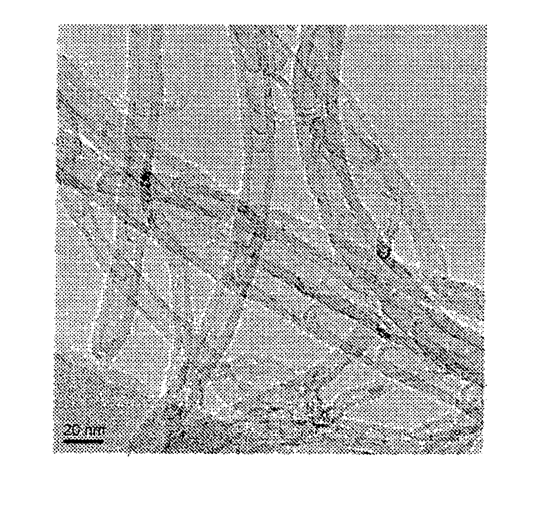
[0018]Whereas existing underfill materials use micro scale particle silica fill, certain embodiments of the present invention use nano scale fill materials (e.g., CNT, organo clay platelets). The nanoscale fill materials increase the modulus above Tg without unduly increasing the viscosity which would be disadvantageous for capillary underfills.

Problems solved by technology

When chips are used in portable electronic gadgets such as smartphones it is to be expected that the chip will be subjected to mechanical shocks because such devices are not always treated as sensitive electronic devices and handled gingerly.
On the contrary it is to be expected that such devices may be dropped or otherwise abused.
Mechanical shocks could cause solder joints in ball grid arrays to fail.

Method used


Image

  • Underfill for high density interconnect flip chips
  • Underfill for high density interconnect flip chips
  • Underfill for high density interconnect flip chips

Examples


examples

[0067]Certain embodiments included a base formulation to which additives were added. While certain ingredients were used in the several examples described below, the invention should not be construed as limited to a particular base formulation. The base formulation used in several examples described below included an epoxy system including Bisphenol F epoxy resin and a polyaromatic amine, a silica fill, a silane coupling agent and a fluoro silicone defoamer. A Comparative Example below explains the procedure for preparing a particular base formulation.

example 1

[0075]Between 1-3% by weight of a quaternary amine substituted clay were added to the composition described in the above Comparative Example prior to the step of mixing. The percentage of clay is relative to the weight of entire formulation. The quaternary amine clay is a product disclosed in U.S. Pat. No. 6,399,690 and sold commercially under the product designation 1.22E, by Nanocor of Hoffman Estates, Illinois. The clay is added together with the other fillers and everything is then milled using the 3 roll mill. During the milling process the clay exfoliates to single platelets. In effect this results in clay platelets functionalized with quaternary amines on the surface. These surface bound quaternary platelet groups are available for reaction with other reactive groups, e.g., epoxy groups of the base formulation (Comparative Example).

example 2

[0076]In addition to the constituents of the comparative example,

[0077]1% of the same quaternary amine substituted clay that was used in example 1; and

[0078]10% of a glycido functionalized branched siloxane, tris(glycidoxypropyldimethylsiloxy)-phenylsilane having the chemical structure shown below were added to the mixture prior to 3 roll milling.

[0079]The percentage of branched siloxane is given in terms of epoxy equivalents.

[0080]There are certain important properties of candidate capillary underfill materials that can be tested. One such property is the modulus of elasticity which is measured as a function of temperature. The modulus of elasticity can be tested by dynamical mechanical analysis (DMA). DMA provides a plot of modulus of elasticity versus temperature. From such plots it is also possible to identify the glass transition temperature. In order to make samples for DMA the compositions prepared as described in the examples described herein are placed between two glass sl...


PUM

PropertyMeasurementUnit
Temperatureaaaaaaaaaa
Percent by massaaaaaaaaaa

Abstract

Underfill materials include inorganic fill materials (e.g., functionalized CNT's, organo clay, ZnO) that are functionalized reactive with other organic constituents (e.g., organics with epoxy groups, amine groups, or PMDA). The underfill materials also beneficially include polyhedral oligomeric silsesquioxane and / or dendritic siloxane groups that are functionalized with a reactive group (e.g., glycidyl) that reacts with other components of an epoxy system of the underfill.

Description

FIELD OF THE INVENTION[0001]The present invention relates generally to an underfill material for use between a semiconductor die and a printed circuit board or package substrate.BACKGROUND ART[0002]The electronic industry has sustained decades of continual reduction of the dimensional scale of integrated circuit features. Both the dimensional scale of the transistors in the integrated circuits and the dimensional scale of the electrical connections to the chip have been reduced. The shrinkage of the scale of transistors allows more functionality to be integrated into a single chip. More chip functionality provides for the plethora of functionality found in modern electronic devices such as smartphones that can play music, play videos, capture images and communicate using a variety of wireless protocols.[0003]More functionality also calls for more electrical connections into the chip and into package in which the chip is contained. A semiconductor is typically provided in a package w...

Claims


Application Information

Patent Timeline
IPC IPC(8): C09J163/00C08K3/22C09J11/04C08K5/1515C08K3/36B82Y30/00
CPCC08G59/306C08G59/3254C08G77/04C08K3/36C08L63/00H01L21/563H01L23/293H01L2924/10253H01L2224/73203C08L2666/22H01L2924/00C08G59/18C08G59/621C08K5/06C08L83/04H01L21/44
Inventor CZUBAROW, PAWELSUZUKI, OSAMUSATO, TOSHIYUKI
Owner NAMICS CORPORATION
Learn More