Inverted multijunction solar cells with group iv alloys

a solar cell and alloy technology, applied in the field of semiconductor devices, can solve problems such as tensors of complex manufacturing

Inactive Publication Date: 2012-07-26
SOLAERO TECH CORP
View PDF4 Cites 37 Cited by
  • Summary
  • Abstract
  • Description
  • Claims
  • Application Information

AI Technical Summary

Benefits of technology

[0012]To satisfy this unmet need, the present disclosure provides methods of fabricating an inverted multijunction solar cell in which the subcells of the solar cell can be grown on a substrate in a “reverse” sequence. For example, higher band gap subcells (i.e. III-V compound semiconductor subcells), which would normally be the “top” subcells facing the solar radiation, are initially grown epitaxially directly on a semiconductor growth substrate, such as for example GaAs or Ge, and such subcells are consequently lattice matched to such substrate. Lower band gap GeSiSn can then be grown over the III-V compound semiconductor subcells at lower deposition temperatures that will not result in degradation of the metastable GeSiSn material. A surrogate substrate or support structure can then be attached or provided over the “bottom” or lower subcell, and the growth semiconductor substrate can subsequently be removed.

Problems solved by technology

Compared to silicon, III-V compound semiconductor multijunction devices have greater energy conversion efficiencies and generally more radiation resistance, although they tend to be more complex to manufacture.

Method used


Image

  • Inverted multijunction solar cells with group iv alloys
  • Inverted multijunction solar cells with group iv alloys
  • Inverted multijunction solar cells with group iv alloys

Examples


first embodiment

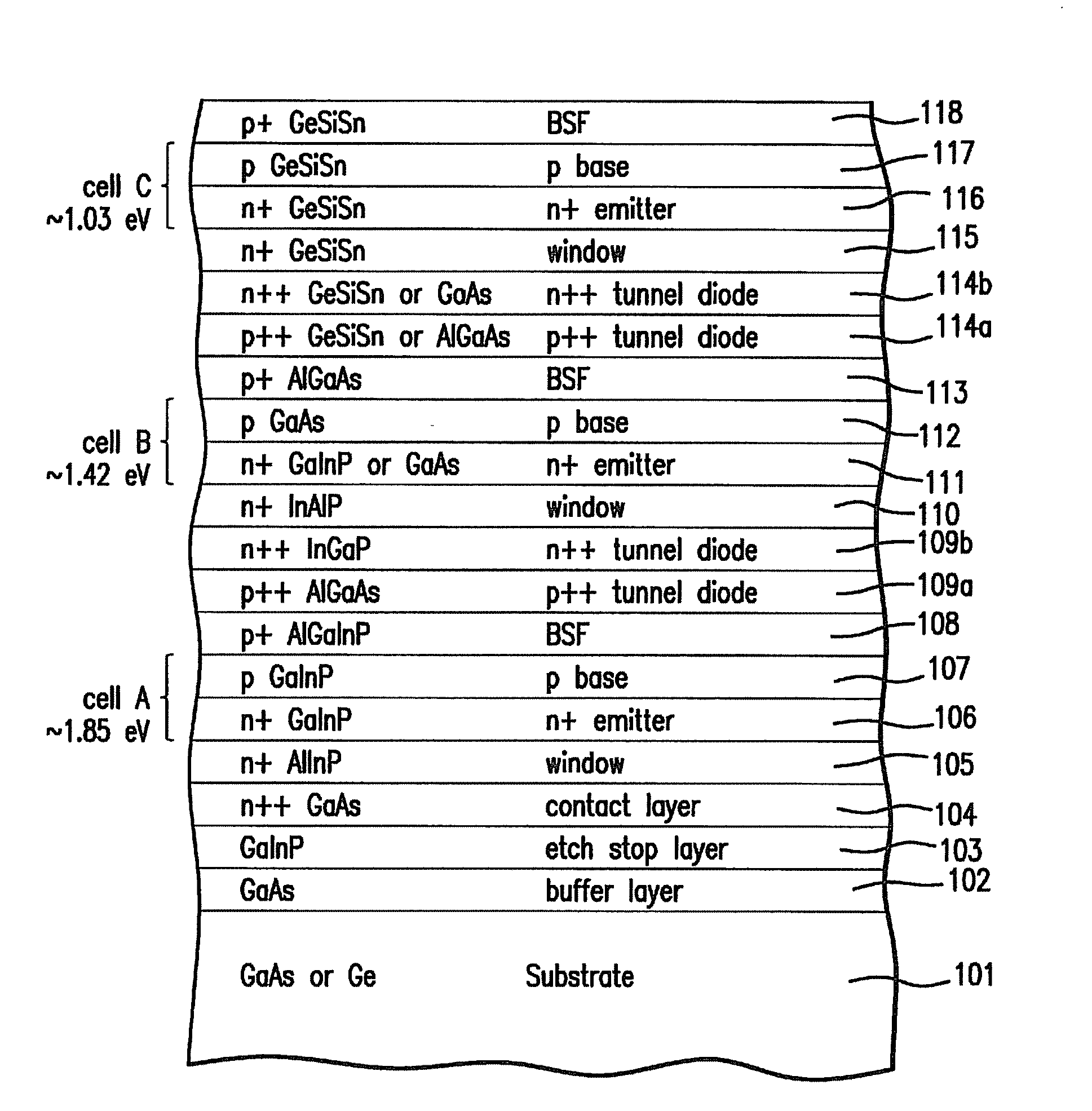
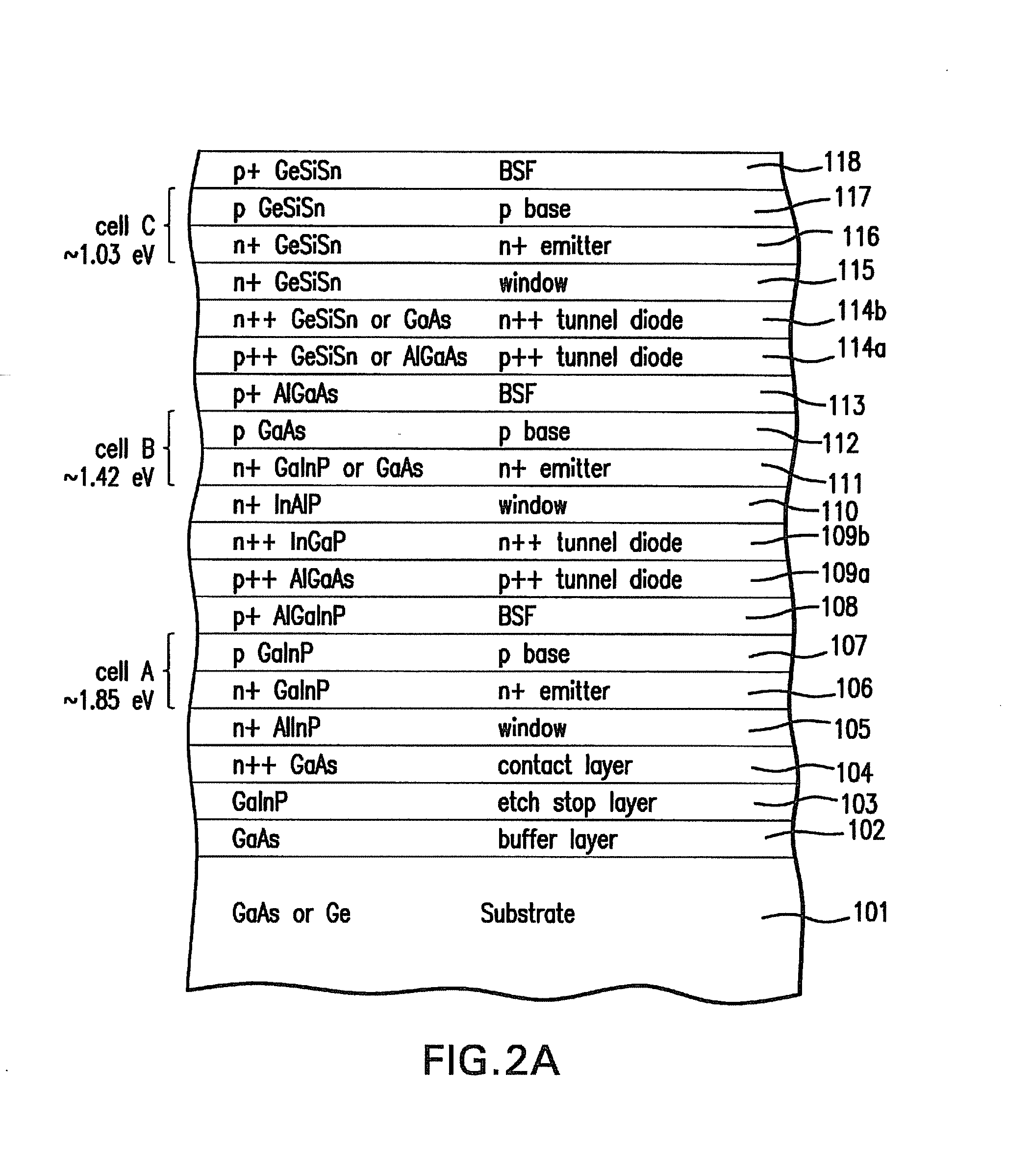
[0051]FIG. 2A depicts the multijunction solar cell according to the present invention after the sequential formation of the three subcells A, B, and C on a GaAs growth substrate. More particularly, there is shown a substrate 101, which is preferably gallium arsenide (GaAs), but may also be germanium (Ge) or other suitable material. For GaAs, the substrate is preferably a 15° off-cut substrate, that is to say, its surface is orientated 15° off the (100) plane towards the (111)A plane, as more fully described in U.S. Patent Application Pub. No. 2009 / 0229662 A1 (Stan et al.). Other alternative growth substrates, such as described in U.S. Pat. No. 7,785,989 B2 (Sharps et al.), may be used as well.

[0052]In the case of a Ge substrate, a nucleation layer (not shown) is deposited directly on the substrate 101. On the substrate, or over the nucleation layer (in the case of a Ge substrate), a buffer layer 102 and an etch stop layer 103 are further deposited. In the case of GaAs substrate, the...

second embodiment

[0071]FIG. 2B depicts the multijunction solar cell according to the present invention after the sequential formation of the four subcells A, B, C, and D on a GaAs growth substrate. More particularly, there is shown a substrate 101, which is preferably gallium arsenide (GaAs), but may also be germanium (Ge) or other suitable material. For GaAs, the substrate is preferably a 15° off-cut substrate, that is to say, its surface is orientated 15° off the (100) plane towards the (111)A plane, as more fully described in U.S. Patent Application Pub. No. 2009 / 0229662 A1 (Stan et al.). Other alternative growth substrates, such as described in U.S. Pat. No. 7,785,989 B2 (Sharps et al.), may be used as well.

[0072]The composition of layers 101 through 117 in the embodiment of FIG. 2B are similar to those described in the embodiment of FIG. 2A, but may have different elemental compositions or dopant concentrations, and will not be repeated here.

[0073]In the embodiment of FIG. 2B, a BSF layer 118, ...

third embodiment

[0147]FIG. 14C is a cross-sectional view of the solar cell of FIG. 12B after the next process step in the present invention in which a cover glass 514 is secured to the top of the cell by an adhesive 513. The cover glass 514 is typically about 4 mils thick and preferably covers the entire channel 510, extends over a portion of the mesa 516, but does not extend to channel 511. Although the use of a cover glass is desirable for many environmental conditions and applications, it is not necessary for all implementations, and additional layers or structures may also be utilized for providing additional support or environmental protection to the solar cell.

[0148]FIG. 14D is a cross-sectional view of the solar cell of FIG. 14A after the next process step in some embodiments of the present invention in which the bond layer, the surrogate substrate 150 and the peripheral portion 517 of the wafer are entirely removed, leaving only the solar cell with the ARC layer 160 (or other layers or stru...


PUM

PropertyMeasurementUnit
band gapaaaaaaaaaa
band gapaaaaaaaaaa
band gapaaaaaaaaaa

Abstract

A method of manufacturing a solar cell comprising providing a growth substrate; depositing on said growth substrate a sequence of layers of semiconductor material forming a solar cell, including at least one subcell composed of a group IV alloy such as GeSiSn; and removing the semiconductor substrate.

Description

[0001]This application is a continuation-in-part of application Ser. No. 12 / 463,205, filed May 8, 2009.BACKGROUND[0002]1. Field of the Invention[0003]The present invention relates to the field of semiconductor devices, and to fabrication processes and devices such as multijunction solar cells based on Group IV alloy semiconductor compounds (e.g., GeSiSn) and hybrid multijunction solar cells that also include different semiconductor compounds (e.g., group III-V semiconductor compounds).[0004]2. Description of Related Art[0005]Solar power from photovoltaic cells, also called solar cells, has been predominantly provided by silicon semiconductor technology. In the past several years, however, high-volume manufacturing of III-V compound semiconductor multijunction solar cells for space applications has accelerated the development of such technology not only for use in space but also for terrestrial solar power applications. Compared to silicon, III-V compound semiconductor multijunction ...

Claims


Application Information

Patent Timeline
Patent Type & Authority Applications(United States)
IPC IPC(8): H01L31/0304H01L31/0312H01L31/18H01L31/02
CPCH01L31/0687H01L31/06875H01L31/0693H01L31/0725Y02E10/544H01L31/1812H01L31/1844H01L31/1852H01L31/0735Y02P70/50
Inventor SHARPS, PAULNEWMAN, FRED
Owner SOLAERO TECH CORP
Why Eureka
Try Eureka