Method of depositing film by atomic layer deposition with pulse-time-modulated plasma

Active Publication Date: 2012-08-02
ASM JAPAN
View PDF6 Cites 328 Cited by
  • Summary
  • Abstract
  • Description
  • Claims
  • Application Information

AI Technical Summary

Benefits of technology

[0008]In at least one of the disclosed embodiments of the present invention, surface potential can effectively be controlled at each cycle during atomic layer deposition. In at least one of the disclosure embodiments, in-plane uniformity of a resultant film can significantly be improved. An embodiment of the present invention provides a method of forming a thin film by alternating multiple times, respectively, a process of adsorbing a precursor onto a substrate and a process of treating the adsorbed surface using a reactant gas and a plasma, wherein the reactant gas is supplied substantially uniformly over the su

Problems solved by technology

To deposit a thick film, it requires a cyclic deposition of at least several hundred times, taking a long time to complete the deposition process.
In the above, since plasma treatment is repeated at least several hundred times, surface potential on the wafer increases as a result of accumulating floating potential on the wafer, leading to the following risks: wafer slip, wafer sticking on a susceptor, and destruction of gate elect loads in a patterned wafer.
However, the above surface potential problems have not been recognized because PE-ALD predominantly targets a thin film and thus, it is believed that surface potential does not increase significantly on the wafer.
Thus, no solutions to the aforementioned problems have been pro

Method used


Image

  • Method of depositing film by atomic layer deposition with pulse-time-modulated plasma
  • Method of depositing film by atomic layer deposition with pulse-time-modulated plasma
  • Method of depositing film by atomic layer deposition with pulse-time-modulated plasma

Examples


example 1

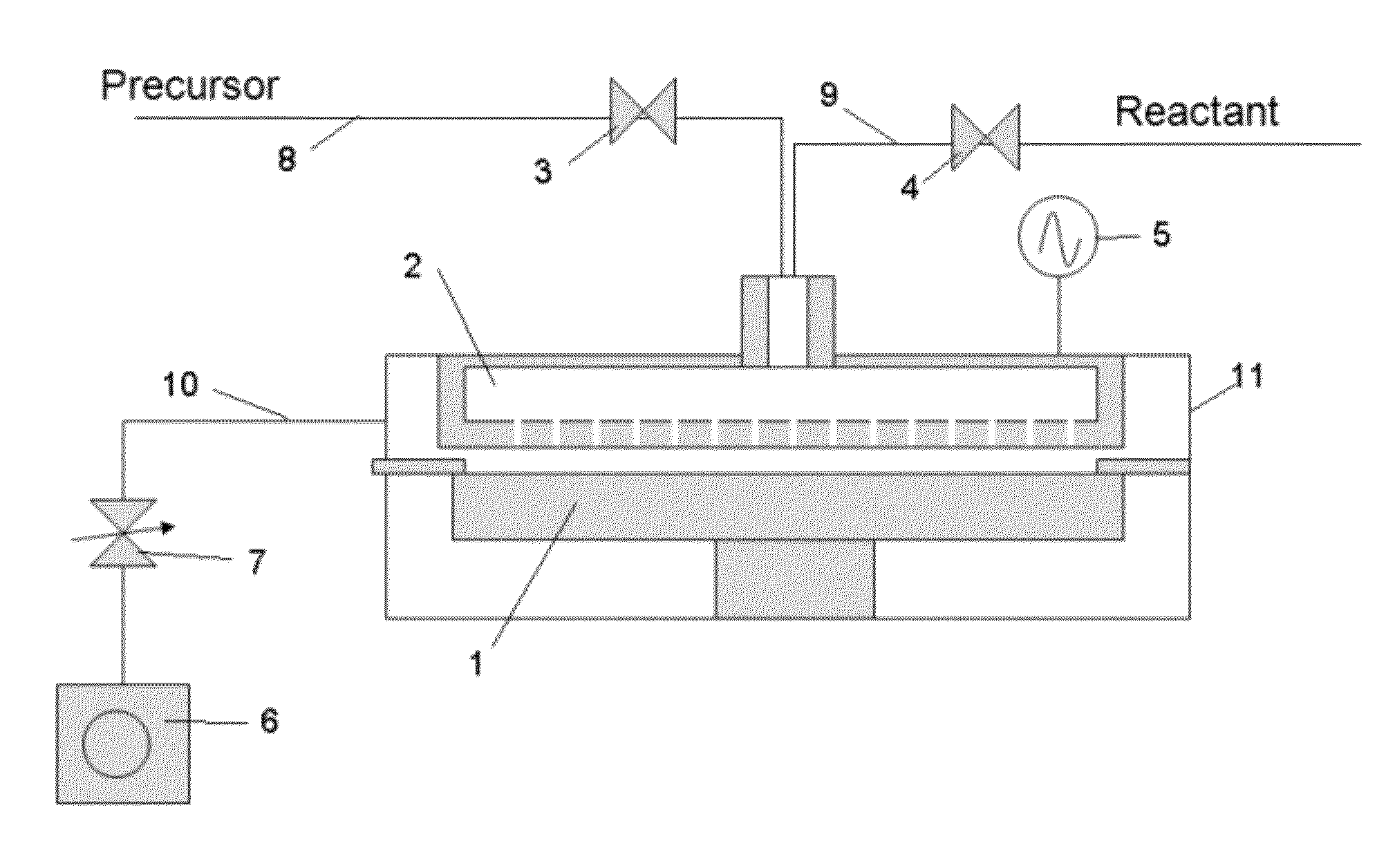
[0048]In this example, the apparatus shown in the schematic diagram of FIG. 1 was used to form a film. This apparatus comprises a reactor 11 which can be retained in a vacuum state, susceptor 1 with heating mechanism used to hold a single wafer on top, shower head 2 which provides a mechanism for supplying gas, RF application mechanism 5 that generates a pulse-time-modulated plasma between the shower head and susceptor, precursor gas supply line 8 equipped with an open / close valve 3 connected to the shower head 2, reactant gas supply line 9 equipped with another open / close valve 4, exhaust line 10 used to exhaust the atmosphere inside the reactor 11, and vacuum pump 6 connected after the exhaust line via a pressure control valve 7, among others. Note that a purge gas line (not illustrated) is also connected to the shower head 2 just like the reactant gas supply line 9.

[0049]A Si wafer (300 mm in diameter) was heated to 70° C., and then N,N,N′,N′-tetraethylsilanediamine (SAM24) being...


PUM

PropertyMeasurementUnit
Fractionaaaaaaaaaa
Fractionaaaaaaaaaa
Timeaaaaaaaaaa

Abstract

A thin film is formed by alternating multiple times, respectively, a process of adsorbing a precursor onto a substrate and a process of treating the adsorbed surface using a reactant gas and a plasma, wherein the reactant gas is supplied substantially uniformly over the substrate, and the plasma is pulse-time-modulated and applied in the process of supplying the reactant gas.

Description

BACKGROUND[0001]1. Field of the Invention[0002]The present invention generally relates to a method of depositing a film by atomic layer deposition (ALD); particularly to a method of depositing a film by ALD with pulse-time-modulated plasma.[0003]2. Description of the Related Art[0004]Plasma Enhanced Atomic Layer Deposition (PE-ALD) is one of the plasma deposition processes. This method forms a film by repeating a process of adsorbing a precursor on a wafer and a process of treating the adsorbed precursor with a reactant gas plasma wherein the reactant gas plasma reacts the precursor adsorbed on the surface, thereby forming an atomic sub-layer on the wafer in each cycle of the repeating processes. To deposit a thick film, it requires a cyclic deposition of at least several hundred times, taking a long time to complete the deposition process. In the above, since plasma treatment is repeated at least several hundred times, surface potential on the wafer increases as a result of accumul...

Claims


Application Information

Patent Timeline
IPC IPC(8): C23C16/515C23C16/40C23C16/56C23C16/36C23C16/455C23C16/30C23C16/34
CPCC23C16/325C23C16/345C23C16/45542C23C16/401C23C16/45536C23C16/40
Inventor UEDA, SHINTARO
Owner ASM JAPAN
Why Eureka
Try Eureka