
Systems and Methods for Susceptor Assisted Microwave Annealing

Inactive Publication Date: 2012-08-02
ARIZONA STATE UNIVERSITY
View PDF11 Cites 26 Cited by
  • Summary
  • Abstract
  • Description
  • Claims
  • Application Information

AI Technical Summary

Benefits of technology

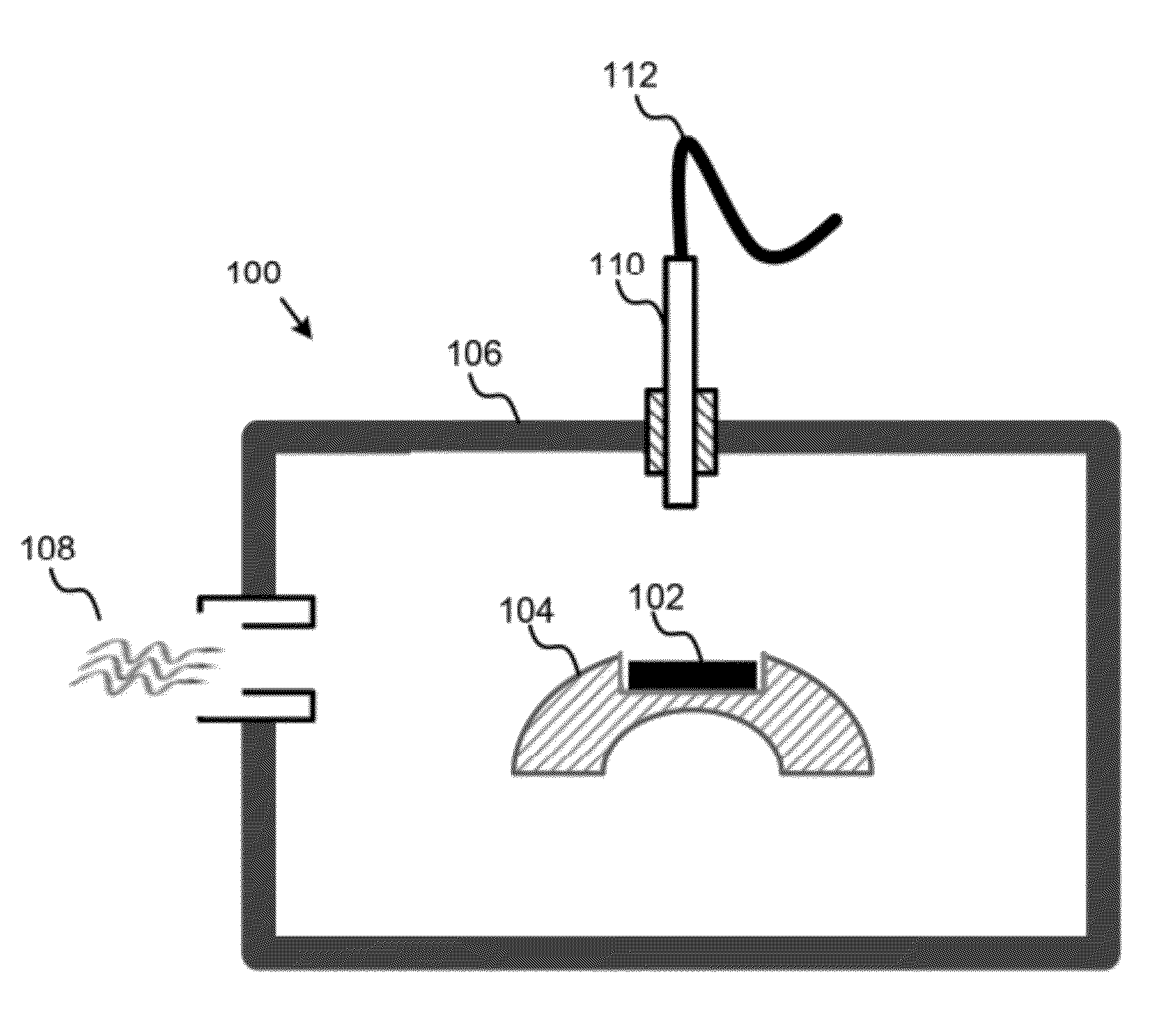
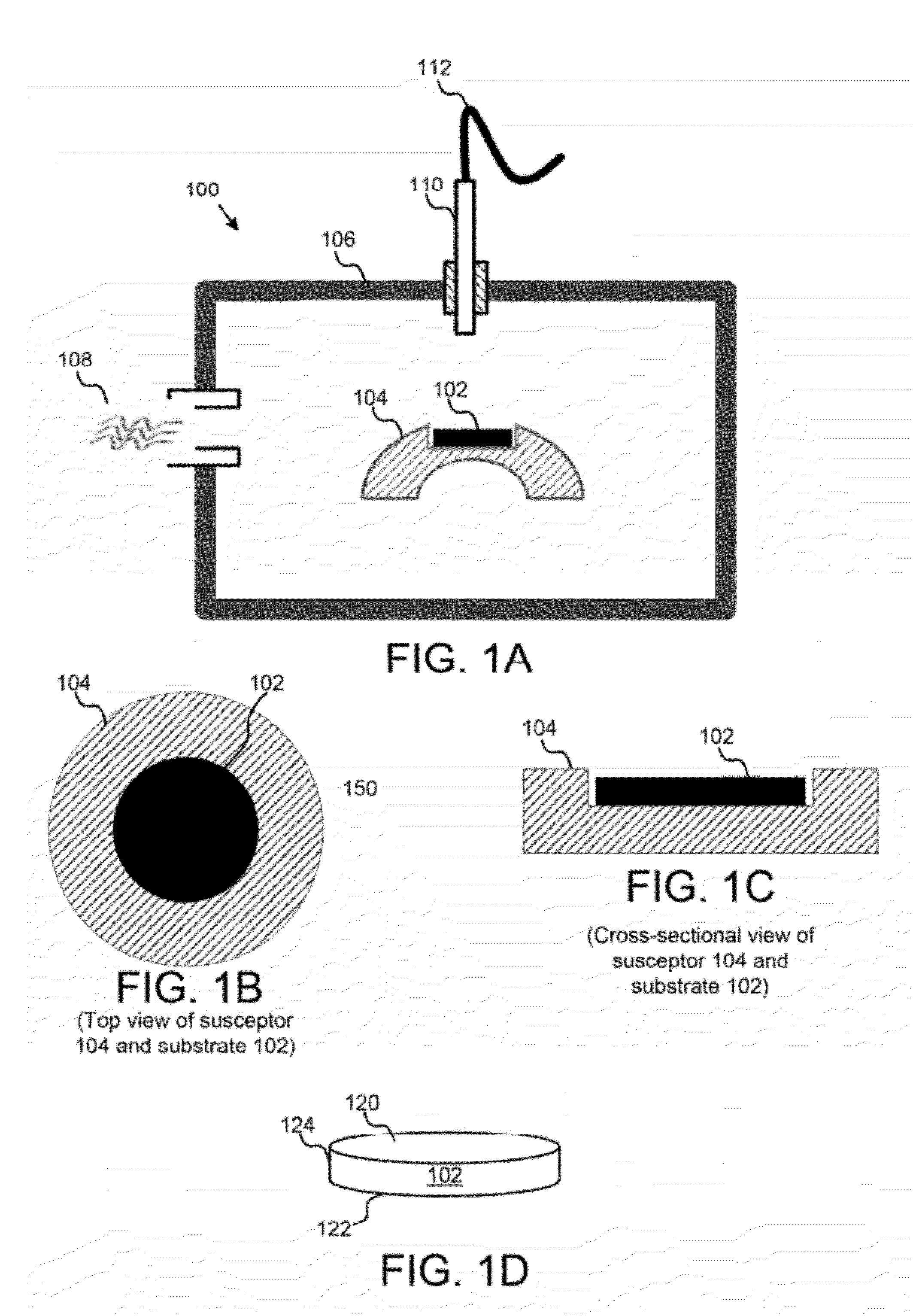
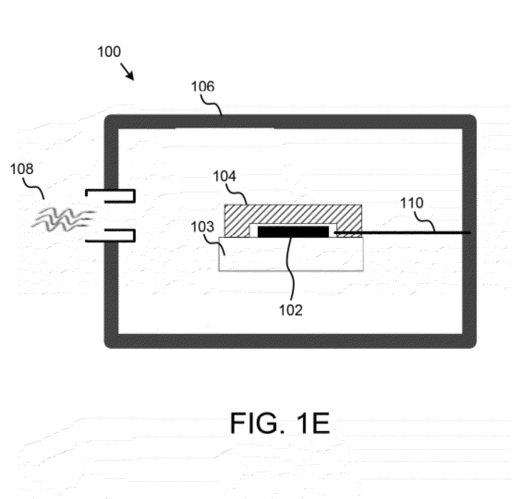
[0007]Systems configured to anneal are disclosed. In some embodiments the system may comprise a microwave emitter configured to emit a microwave at a single frequency during an anneal time. In some embodiments, the system may further comprise an anneal unit having

Problems solved by technology

But doping may damage the surface of these already thin films and may amorphize them.
Post implant processes should not allow for extensive dopant diffusion.
MIC may crystallize substrates (e.g., Si) at lower temperatures and shorter duration, but runs the risk of contamination and disintegration of the film.
Laser annealing, though used earlier extensively, provides uneven heating of the sample.
Traditional annealing processes, such as vacuum annealing, for metal alloy thin films suffer from poor performance and a very long anneal time is required.

Method used


Image

  • Systems and Methods for Susceptor Assisted Microwave Annealing
  • Systems and Methods for Susceptor Assisted Microwave Annealing
  • Systems and Methods for Susceptor Assisted Microwave Annealing

Examples


example 1

[0052]Microwave annealing of different dosage arsenic implanted Si samples was done in a single-frequency (2.45 GHz), 2.8×104 cm3 cavity applicator microwave system equipped with a 1300 Watt magnetron source, with annealing times of 40, 70, and 100 seconds for each sample type. A Raytek Compact MID series pyrometer with a spectral response of 8-14 μm was used to monitor the near surface temperature. The emissivity for the samples was adjusted by careful calibration of the temperature read by the pyrometer against the temperature monitored by a thermocouple. For the arsenic implanted samples, the surface temperatures ranged from 620-680° C. FIG. 2B shows a typical plot of temperature of two samples versus anneal time for 1×10¹⁵ As+ cm−2 samples which were microwave annealed for 100 s. The anneal time is defined as the duration between when the microwave is switched on and when the microwave is turned off.

[0053]For the first sample, the annealing of the samples was assisted by silicon...

example 2

[0065]Two different annealing methods, microwave annealing and vacuum thermal annealing, were used to anneal Ag—Cu thin films, which can serve as a possible and reliable interconnect system. The thin films of Ag—Cu used here were deposited by co-sputtering. A sputter target of pure Ag and pure Cu were used. The base pressure of the sputter system before each deposition was approximately 1×10⁻⁷ Torr. The deposition was performed using pure Ar gas (99.999%) at a pressure of 10 mTorr. The dc power for Ag deposition was fixed at 50 W; whereas, the dc power for Cu deposition was varied. The thickness and composition of the Ag—Cu alloy films were determined using Rutherford backscattering spectrometry (RBS) with a General Ionex Tandetron accelerator. Samples were analyzed in a vacuum of less than 10−6 Torr using a 2.0 MeV He ion beam and the sample tilt angle was 8 degrees. The RUMP computer-simulation program was used to determine composition and thicknesses.

[0066]For microwave annealing...


PUM


Abstract

Systems and methods for microwave annealing are disclosed. In some embodiments, the system may comprise a microwave emitter configured to emit a microwave at a single frequency during an anneal time. In some embodiments, the system may further comprise an anneal unit to be annealed, the anneal unit having a top side, a bottom side, and one or more edge sides. In some embodiments, the system may further comprise a susceptor configured to absorb microwave energy, where the susceptor is adjacent to the edge side and at the bottom side of the anneal unit.

Description

CROSS-REFERENCE TO RELATED APPLICATIONS[0001]This application claims priority to U.S. Provisional Application No. 61 / 438,515 filed Feb. 1, 2011, the entire contents of which are incorporated herein by reference.BACKGROUND OF THE INVENTION[0002]1. Field of the Invention[0003]This invention relates to semiconductors and more particularly relates to systems and methods for susceptor assisted microwave annealing of semiconductors.[0004]2. Description of the Related Art[0005]Thin crystalline silicon (Si) films have gained increased importance in the semiconductor industry since the advent of the thin film transistors (TFTs) in the 1980s. The crucial regions such as drain / source in ultra-shallow transistors may too require thin crystalline layers that are doped, in order to provide the necessary conductivity in these regions. But doping may damage the surface of these already thin films and may amorphize them. Post implant processes should not allow for extensive dopant diffusion. It may ...

Claims


Application Information

Patent Timeline
IPC IPC(8): H01L21/263H05B6/64
CPCH05B6/6491H01L21/2636H05B6/80H01L21/324
Inventor ALFORD, TERRY L.
Owner ARIZONA STATE UNIVERSITY
Learn More