Self-bypass diode function for gallium arsenide photovoltaic devices

a photovoltaic device and self-bypass technology, applied in the field of photovoltaic devices, can solve the problems of severe power reduction, affecting the performance of the entire string or module, and shading on parts of the solar panel, and achieve the effect of greater efficiency and flexibility

Active Publication Date: 2012-08-09
ALTA DEVICES INC
View PDF14 Cites 43 Cited by
  • Summary
  • Abstract
  • Description
  • Claims
  • Application Information

AI Technical Summary

Benefits of technology

[0014]The embodiments of photovoltaic devices described herein provide a bypass function in a gallium arsenide photovoltaic cell to allow bypass current to flow in mismatched conditions such as shading of some cells in a series string. This self-bypass functionality allows protection of cells while avoiding the need for separate or distinct bypass diodes to be connected to the cells. Such innovations can allow for greater efficiency and flexibility in resulting photovoltaic devices and in forming such when compared to conventional solar cell fabrication processes.

Problems solved by technology

One issue with the use of photovoltaic devices such as solar panels is the problem of shading on portions of the solar panel.
However, a portion of these cells may get shaded from sunlight during operation, which affects the performance of the entire string or module.
Thus, in a series connected configuration with current mismatch, severe power reductions can occur if the poor cell produces less current.
If the configuration is operated at short circuit or low voltages, the highly localized power dissipation in the shaded cell can cause local “hot spot” heating, avalanche breakdown, and irreversible damage to one or more of the solar cells and to the module.
Although bypass diodes are effective in reducing the destructive effects of mismatches in solar cells due to shading, they are an additional component that must be fabricated for solar cells and thus add to the cost and time of production of solar panels.
Furthermore, the bypass diodes must be integrated into a solar cell design, which may be complex and difficult to accomplish.
These factors add to the currently higher cost of producing solar cells, may reduce the capability of solar cells in becoming a mainstream energy source, and may limit the applications to which solar cells may be suited.

Method used


Image

  • Self-bypass diode function for gallium arsenide photovoltaic devices
  • Self-bypass diode function for gallium arsenide photovoltaic devices
  • Self-bypass diode function for gallium arsenide photovoltaic devices

Examples


Embodiment Construction

[0025]Embodiments of the invention generally relate to photovoltaic devices and processes, and more specifically to photovoltaic cells and the fabrication processes for forming such photovoltaic cells. The following description is presented to enable one of ordinary skill in the art to make and use the inventions and is provided in the context of a patent application and its requirements. Various modifications to the preferred embodiment and the generic principles and features described herein will be readily apparent to those skilled in the art. Thus, the present invention is not intended to be limited to the embodiment shown but is to be accorded the widest scope consistent with the principles and features described herein.

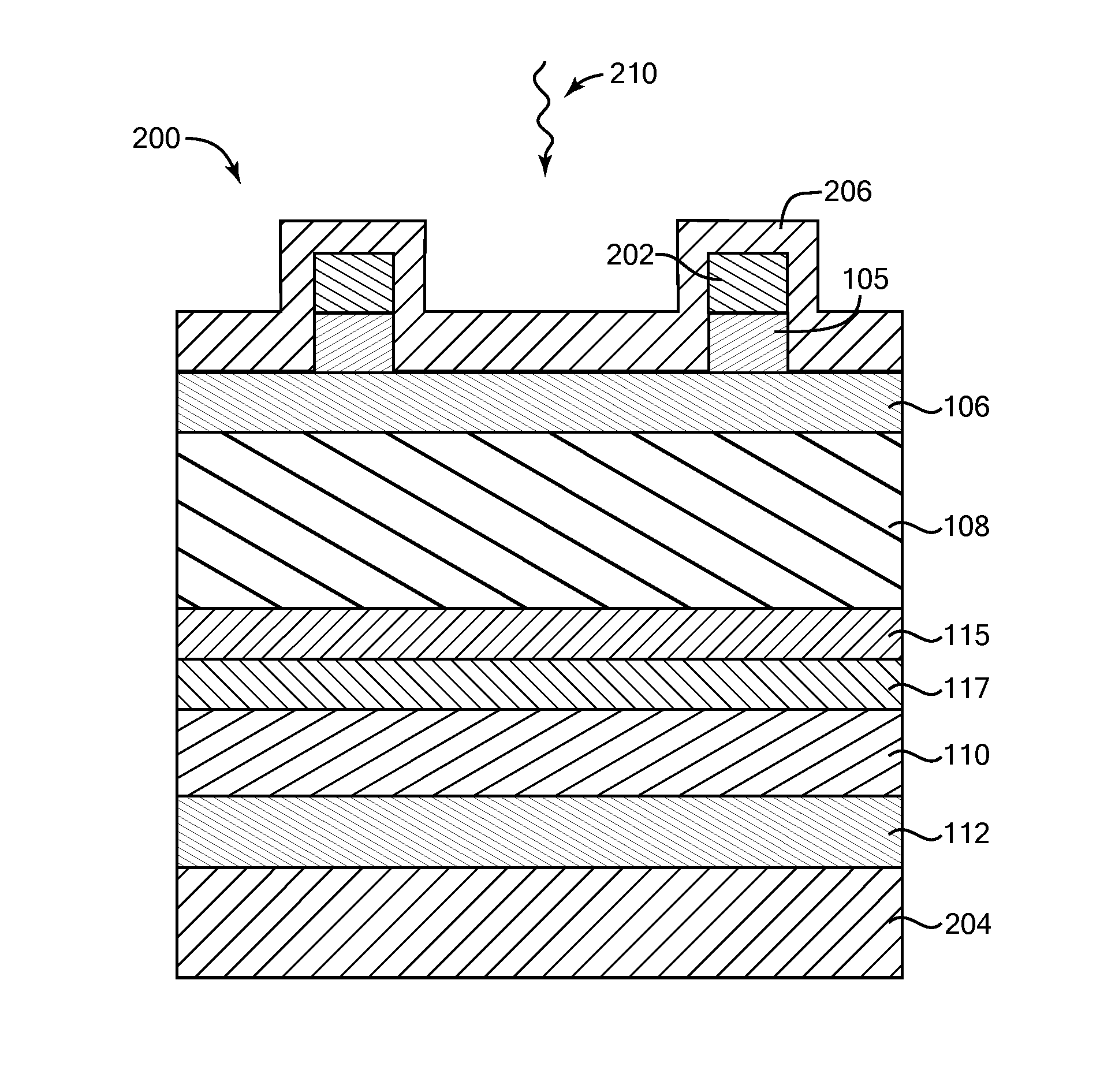
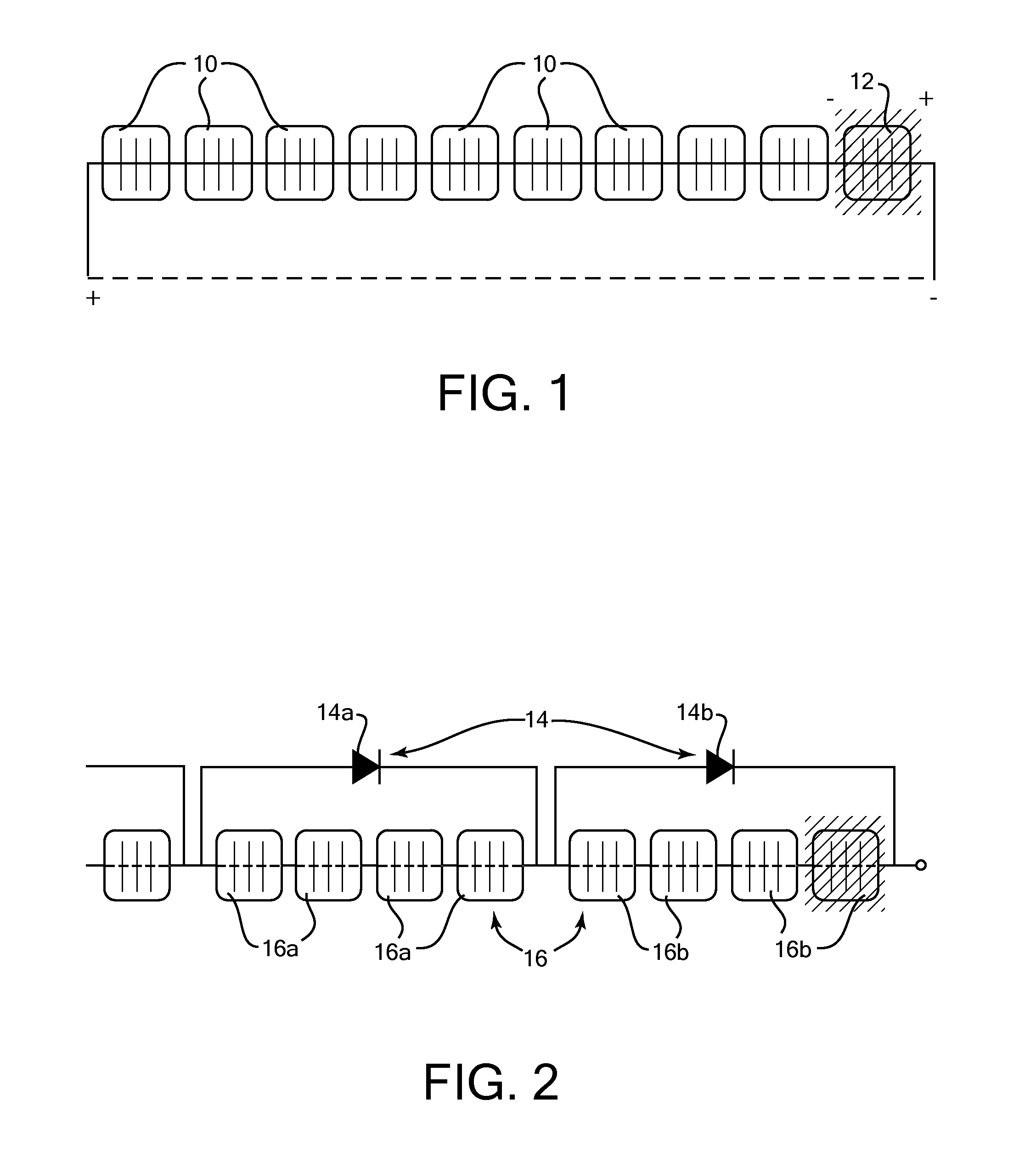
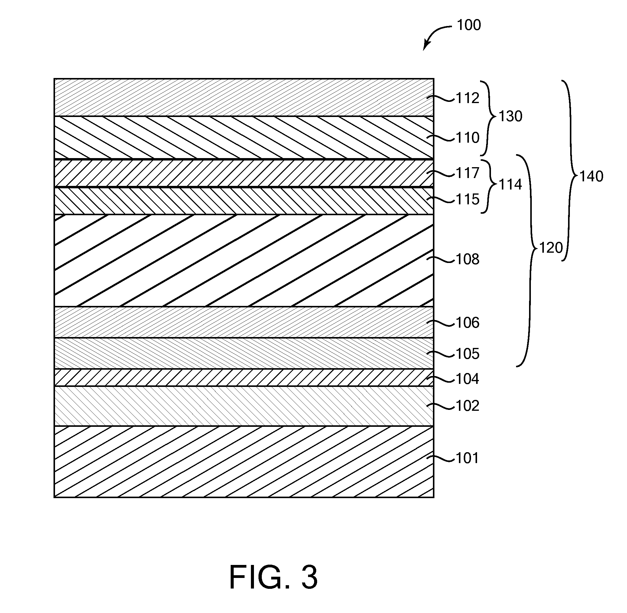
[0026]Embodiments of photovoltaic devices described herein provide a bypass function in a photovoltaic cell to allow bypass current to flow in mismatched conditions, such as shading of some solar cells in a series string. The self-bypass functionality provided i...


PUM


Abstract

Embodiments of the invention generally relate to photovoltaic devices. In one embodiment, a method for forming a gallium arsenide based photovoltaic device includes providing a semiconductor structure, the structure including an absorber layer comprising gallium arsenide. A bypass function is provided in a p-n junction of the semiconductor structure, where under reverse-bias conditions the p-n junction breaks down in a controlled manner by a Zener breakdown effect.

Description

BACKGROUND OF THE INVENTION[0001]1. Field of the Invention[0002]Embodiments of the invention generally relate to photovoltaic devices, such as solar cells, and methods for fabricating such photovoltaic devices.[0003]2. Description of the Related Art[0004]As fossil fuels are being depleted at ever-increasing rates, the need for alternative energy sources is becoming more and more apparent. Energy derived from wind, from the sun, and from flowing water offer renewable, environment-friendly alternatives to fossil fuels, such as coal, oil, and natural gas. Being readily available almost anywhere on Earth, solar energy is becoming a viable alternative.[0005]To harness energy from the sun, the junction of a solar cell absorbs photons to produce electron-hole pairs, which are separated by the internal electric field of the junction to generate a voltage, thereby converting light energy to electric energy. The generated voltage can be increased by connecting solar cells in series, and the c...

Claims


Application Information

Patent Timeline
Patent Type & Authority Applications(United States)
IPC IPC(8): H01L31/06H01L31/0352
CPCH01L27/142Y02E10/544H01L31/03046H01L31/0304H01L31/02H01L31/0352H01L31/0693H01L31/1876H01L31/0735H01L31/0443Y02P70/50H01L31/06H01L31/072H01L31/04
Inventor NIE, HUIKAYES, BRENDAN M.KIZILYALLI, ISIK C.
Owner ALTA DEVICES INC
Why Eureka
Try Eureka