Method of Depositing Dielectric Film by ALD Using Precursor Containing Silicon, Hydrocarbon, and Halogen
- Summary
- Abstract
- Description
- Claims
- Application Information
AI Technical Summary
Benefits of technology
Problems solved by technology
Method used
Image
Examples
example
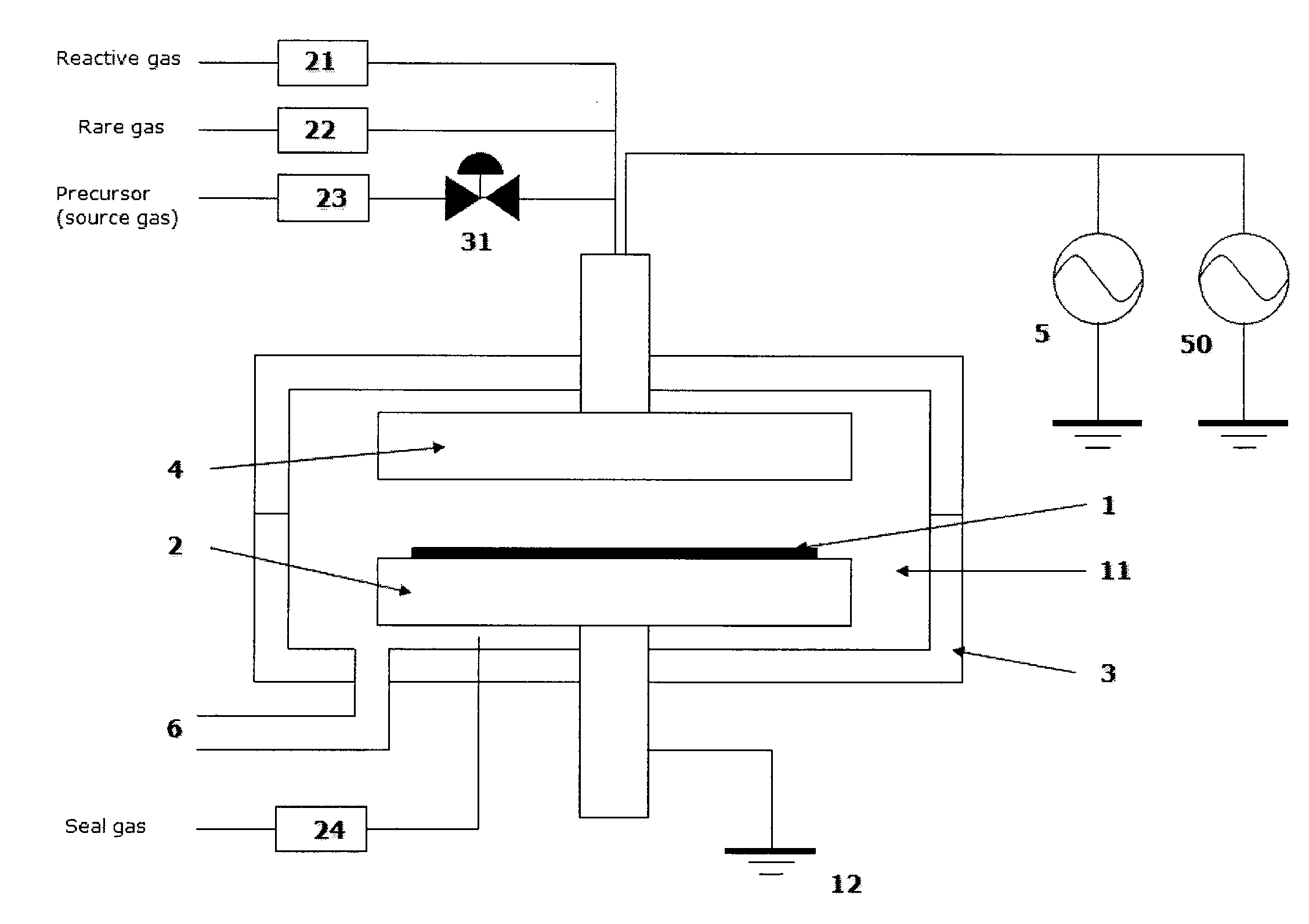
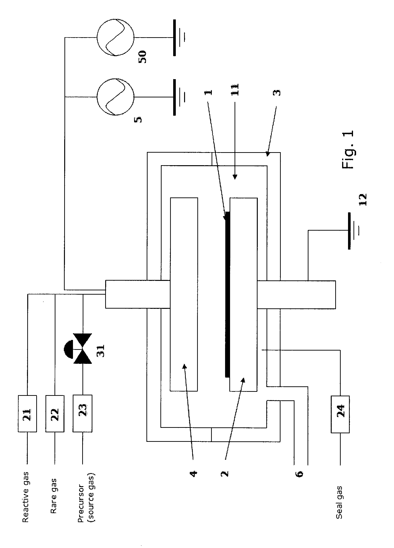
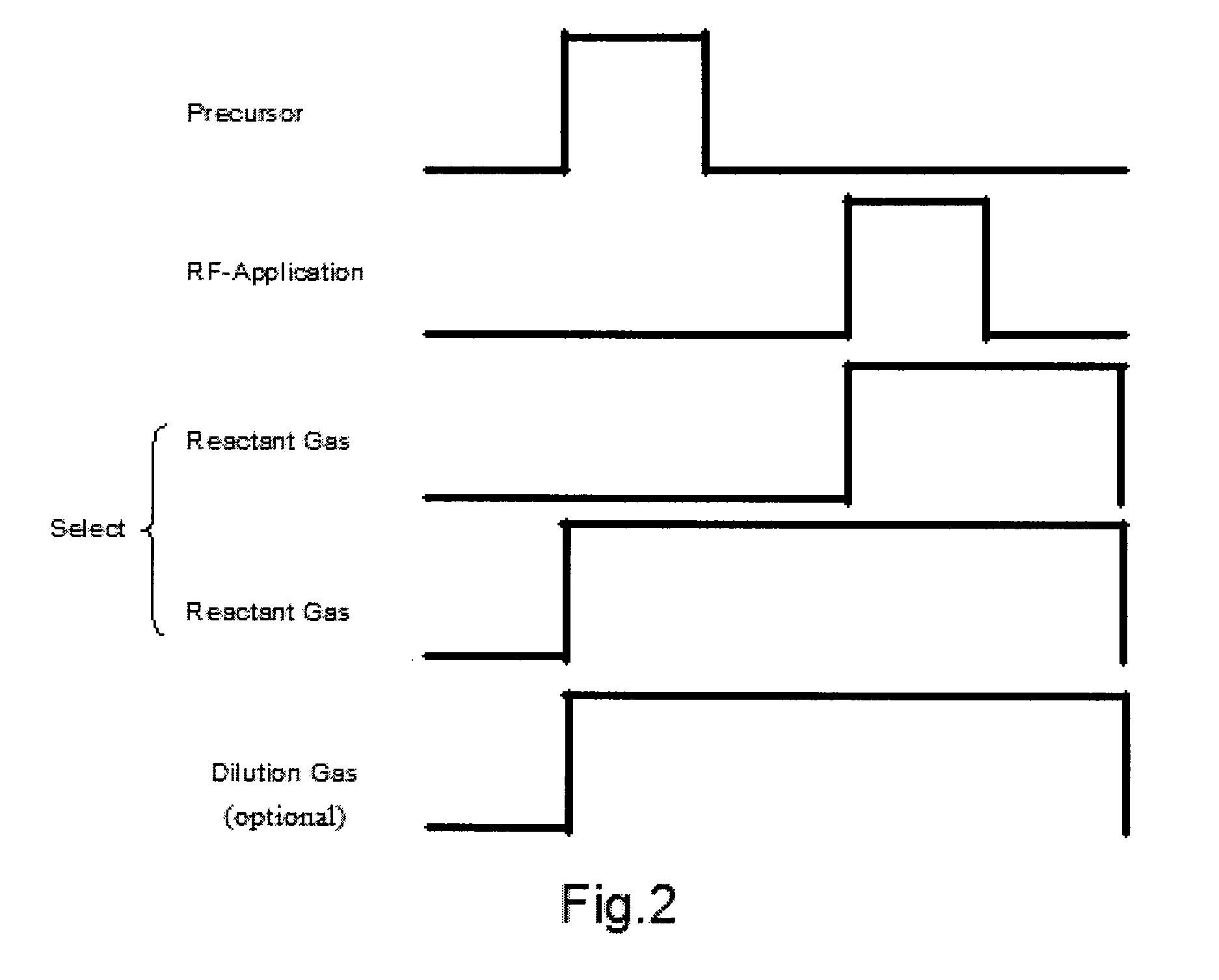
[0092]A dielectric film was formed on a 300-mm substrate having a patterned surface having an aspect ratio of about 2 and an opening width of about 50 nm under the condition shown below using Sequences 1 to 3 illustrated in FIGS. 2 to 4 and the PE-ALD apparatus illustrated in FIG. 1. The thickness of film was 30 nm for evaluating film properties.
[0093]Sequence 1:
[0094]Precursor inflow pressure: 133-1333 Pa (It depended on vapor pressure of precursor)
[0095]Carrier gas (Ar) flow: 2000 sccm
[0096]Reactant gas flow: 2000 sccm
[0097]Purge gas: He
[0098]Purge gas flow (continuous): 500 sccm
[0099]RF frequency: 13.56 MHz
[0100]Precursor supply time: 0.1-1 sec supply (It depended on vapor pressure of precursor)
[0101]Purge time: 1 sec
[0102]Reactant gas supply time (continuous): 2000 sccm
[0103]Purge time: 1 sec
[0104]RF Plasma exciting time: 1 or 3 (longer time for SiN) sec excite
[0105]Sequence 2
[0106]Same as in Sequence 1 except:
[0107]Purge time between reactant gas A pulse and reactant gas B puls...
PUM
| Property | Measurement | Unit |
|---|---|---|
| Temperature | aaaaa | aaaaa |
| Temperature | aaaaa | aaaaa |
| Frequency | aaaaa | aaaaa |
Abstract
Description
Claims
Application Information


