
Semiconductor Powder and Method for Producing the Same

a technology of semiconductors and powders, applied in the field of semiconductor powders, can solve problems such as unsuitable industrial us

Inactive Publication Date: 2012-08-30
MITSUI MINING & SMELTING CO LTD
View PDF4 Cites 15 Cited by
  • Summary
  • Abstract
  • Description
  • Claims
  • Application Information

AI Technical Summary

Benefits of technology

[0008]The inventors have currently found that it is possible to produce, in a simple way according to wet synthesis, a high-grade semiconduct...

Problems solved by technology

However, these compounds are merely those obtained as a single crystal, and are not suitable for industrial utilization not only because a long time is required for forming a single crystal but also because a coarse single crystal needs to be elaborately pulverized and processed to form a powder having desired particle diameters for industrial utilization.

Method used


Image

  • Semiconductor Powder and Method for Producing the Same
  • Semiconductor Powder and Method for Producing the Same
  • Semiconductor Powder and Method for Producing the Same

Examples


example 1

Preparation of CZTS Semiconductor Powder

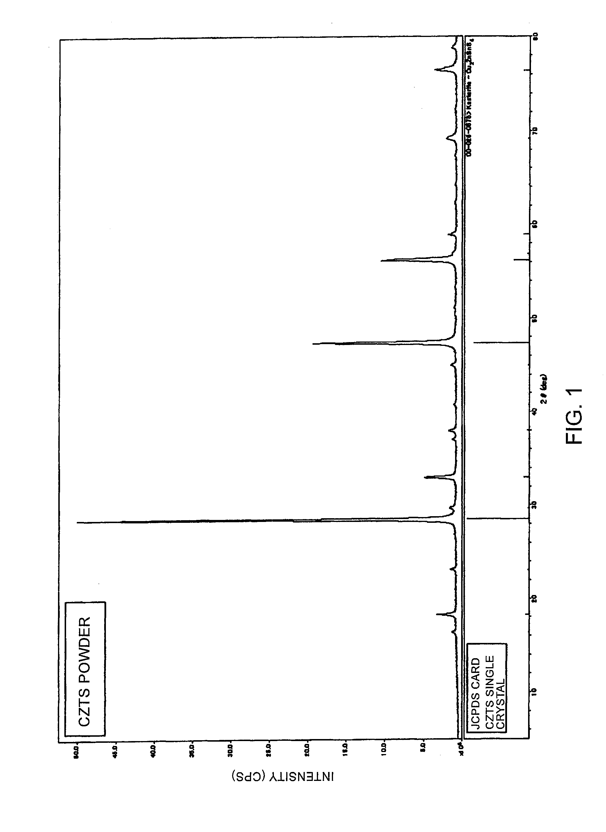
[0058]22 ml of tin sulfate aqueous solution of pH 1.1 containing 5.06 g of tin sulfate dissolved therein was added to 40 ml of 20 mass % ammonium sulfide aqueous solution of pH 10.0, and was then stirred for 15 minutes to obtain a mixture liquid of pH 9.8. Subsequently, 14 ml of zinc sulfate aqueous solution of pH 4.5 containing 6.77 g of zinc sulfate heptahydrate dissolved therein was added to the mixture liquid, and was then stirred for 15 minutes to obtain a mixture liquid having a pH of 9.6. Further, to this mixture liquid, 80 ml of copper sulfate aqueous solution of pH 3.5 containing 11.76 g of copper sulfate pentahydrate dissolved therein was added to obtain a mixture liquid of pH 9.3. The mixture liquid thus obtained was subjected to neutralization by adding 2.8 ml of concentrated sulfuric acid, to obtain a preparatory liquid of pH 7.5. The Cu:Zn:Sn:S ratio in the preparatory liquid was about 2:1:1:5. The mixture liquid was stirred for ...

example 2

Particle-Size Control of CZTS Semiconductor Powder

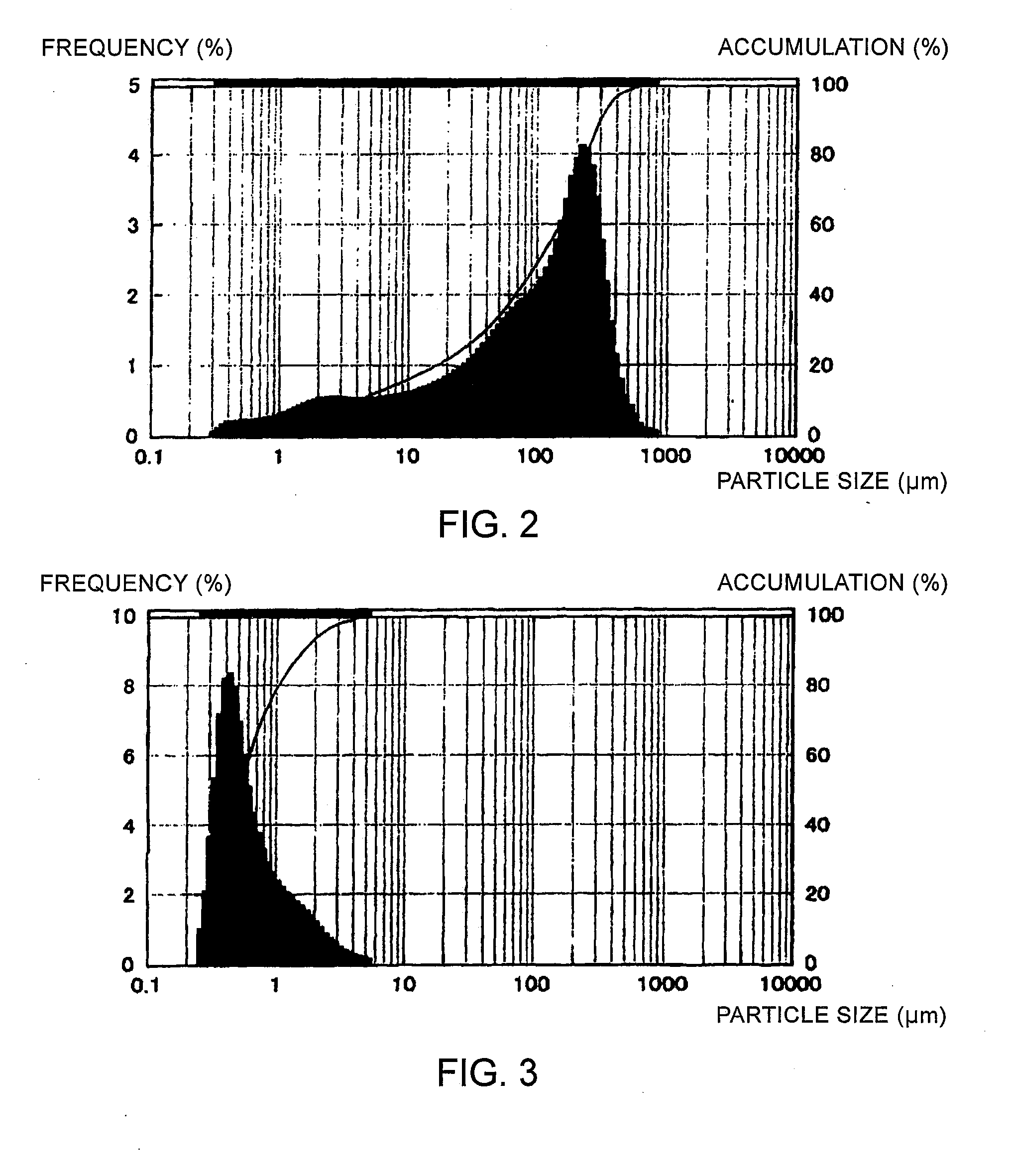
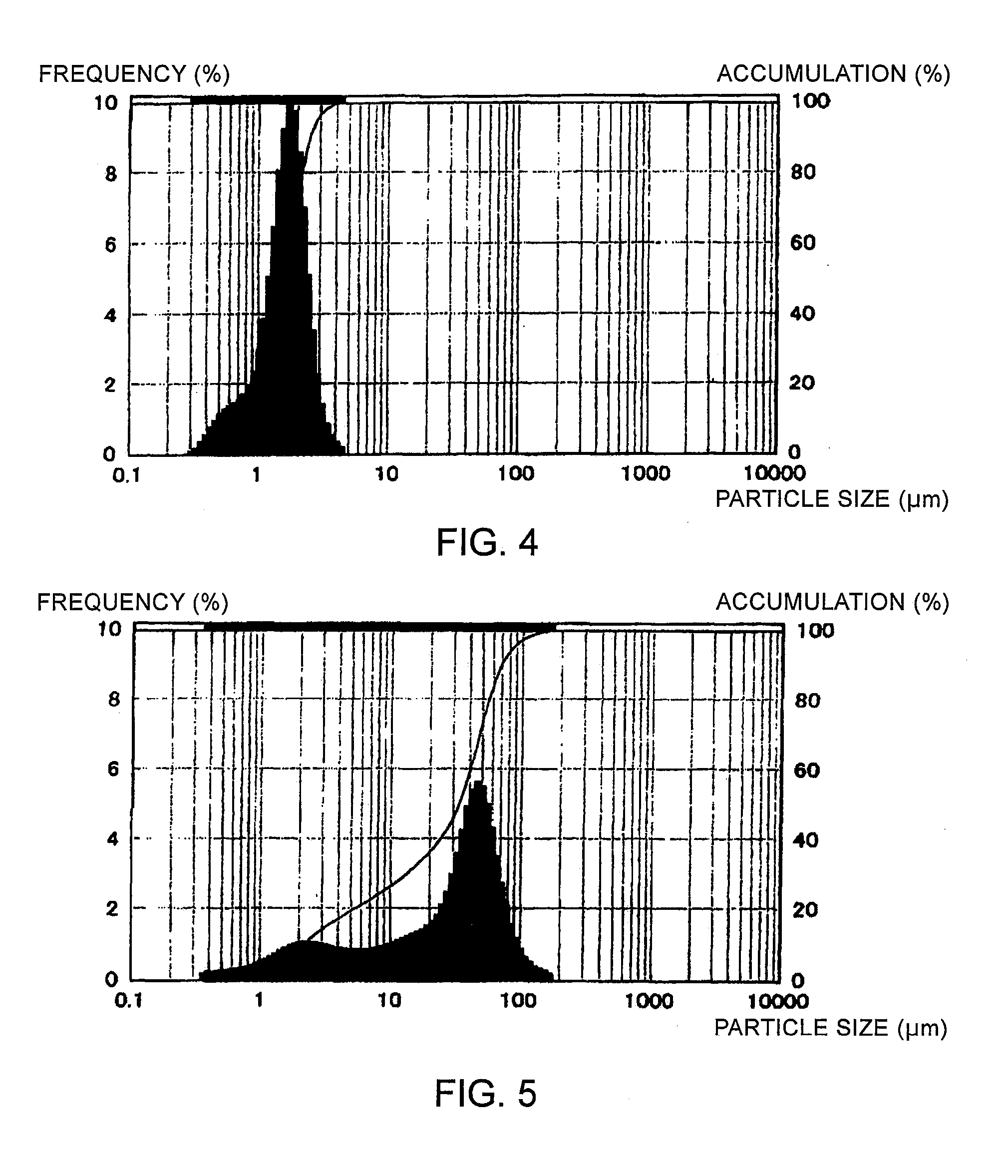
[0060]The CZTS semiconductor powder obtained in Example 1 was subjected to either one of the following steps to control the particle size, followed by the measurement of the particle size distribution using a laser diffraction / scattering particle size distribution measurement device (Microtrac MT3200 (WET), Nikkiso Co., Ltd.):

[0061]Step 1: the powder was pulverized by a jet mill (KJ-25, Kurimoto, Ltd.) under the conditions of a classification rotor frequency of 300 Hz and a pulverization pressure of 0.5 MPa, and then recovered by a bag filter;

[0062]Step 2: the powder was pulverized by a jet mill (KJ-25, Kurimoto, Ltd.) under the conditions of a classification rotor frequency of 300 Hz and a pulverization pressure of 0.5 MPa, and then recovered by a cyclone separator; or

[0063]Step 3: the powder was passed through a sieve with apertures of 75 μm while being crumbled in a mortar.

[0064]The particle size distribution data obtained for the...

example 3

Preparation of CZTS Semiconductor Powder Having Various Cu:Zn:Sn:S Ratios

[0065]Preparation of each Cu2ZnSnS4 (CZTS) semiconductor powder and XRD analysis were conducted in the same manner as in Example 1 to obtain XRD charts shown in FIGS. 6 and 7, except that each additive amount of the raw materials was adequately changed so that the Cu:Zn:Sn:S ratio in the preparatory liquid could be about 2:1:1:4 and about 2:1:1:10 respectively. FIG. 7 is an enlarged chart showing the circled portions in FIG. 6. FIGS. 6 and 7 also show, for reference, the XRD chart obtained on the sample of the Cu:Zn:Sn:S ratio of about 2:1:1:5 obtained in Example 1. As apparent from FIGS. 6 and 7, the sample resulting from the preparatory liquid having the Cu:Zn:Sn:S ratio of about 2:1:1:5 exhibited roughly the same peak behavior over the entire diffraction angles as the sample of the Cu:Zn:Sn:S ratio of about 2:1:1:5 in Example 1. In contrast, the sample resulting from the preparatory liquid having the Cu:Zn:S...


PUM

PropertyMeasurementUnit
Acidityaaaaaaaaaa
Particle sizeaaaaaaaaaa
Electrical conductanceaaaaaaaaaa

Abstract

The present invention provides a semiconductor powder composed of Cu-M-Sn—S in a single phase wherein M is at least one selected from the group consisting of Zn, Co, Ni, Fe and Mn, the powder being obtained by wet synthesis, and a method for producing this semiconductor powder. According to the present invention, it is possible to provide, in a simple way, a high-grade semiconductor powder composed of a single-phase Cu-M-Sn—S such as CZTS.

Description

CROSS-REFERENCE TO RELATED APPLICATION[0001]This application claims priority to Japanese Patent Application No. 2009-183412 filed on Aug. 6, 2009, the entire disclosure of which is incorporated herein by reference.TECHNICAL FIELD[0002]The present invention relates to a semiconductor powder having a composition of Cu-M-Sn—S wherein M is at least one selected from the group consisting of Zn, Co, Ni, Fe and Mn and a method for producing this semiconductor powder.BACKGROUND ART[0003]In recent years, there has been an increasing expectation for Cu2ZnSnS4 (CZTS) as a next-generation semiconductor. This CZTS is known as having benefits such that abundant amounts of the constituent elements exist on the earth, that CZTS has a bandgap energy (1.4 to 1.5 eV) suitable for solar cells, and that CZTS includes no environmentally burdening elements or rare elements. For example, CZTS in a thin film form has been proposed in solar cell applications (Patent Literatures 1 and 2).[0004]In addition, no...

Claims


Application Information

Patent Timeline
IPC IPC(8): H01B1/10B32B5/16C01G19/00
CPCC01G1/12Y10T428/2982C01G45/006C01G49/009C01G51/006C01G53/006C01P2002/72C01P2004/62C01P2006/40H01L21/02557H01L21/02568H01L21/02601C01P2002/74C01P2004/52C01P2004/61C01G19/006
Inventor MITSUMOTO, TETSUYAANNO, YUICHI
Owner MITSUI MINING & SMELTING CO LTD
Learn More