Semiconductor device manufacturing method and computer-readable storage medium

a manufacturing method and semiconductor technology, applied in solid-state devices, electric discharge tubes, coatings, etc., can solve the problems of deteriorating manufacturing efficiency, difficult to appropriately form a good step-shaped structure, and a large number of processes that need to be performed, so as to achieve efficient step-shaped structure

Active Publication Date: 2012-09-06
TOKYO ELECTRON LTD
View PDF5 Cites 349 Cited by
  • Summary
  • Abstract
  • Description
  • Claims
  • Application Information

AI Technical Summary

Benefits of technology

[0008]In accordance with an illustrative embodiment, it is possible to effic

Problems solved by technology

However, in the aforementioned semiconductor device manufacturing process for forming the step-shaped structure in the multilayer film formed by alternately layering two kinds of layers each having a different permittivity, for example, an insulating film and a cond

Method used


Image

  • Semiconductor device manufacturing method and computer-readable storage medium
  • Semiconductor device manufacturing method and computer-readable storage medium
  • Semiconductor device manufacturing method and computer-readable storage medium

Examples


Embodiment Construction

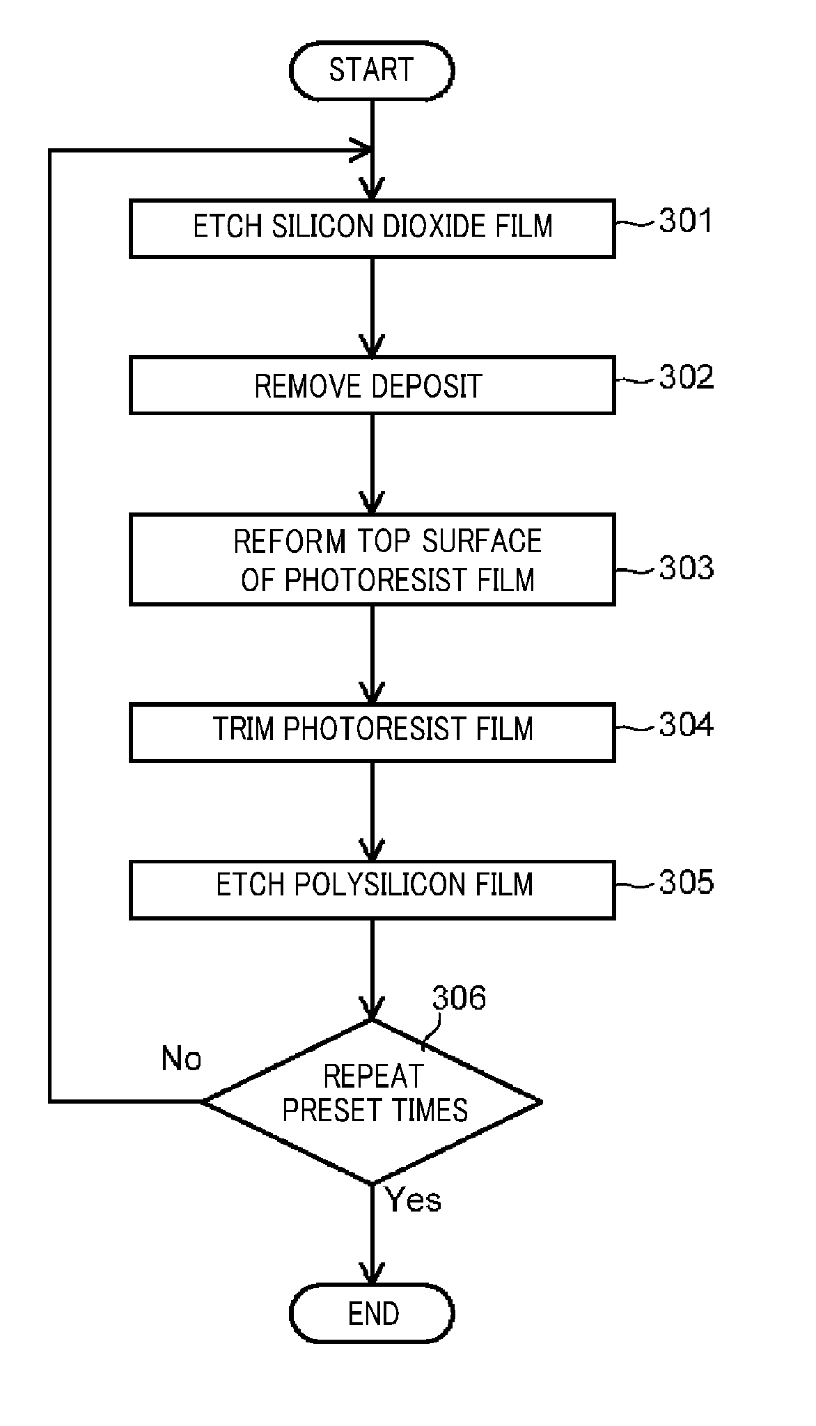
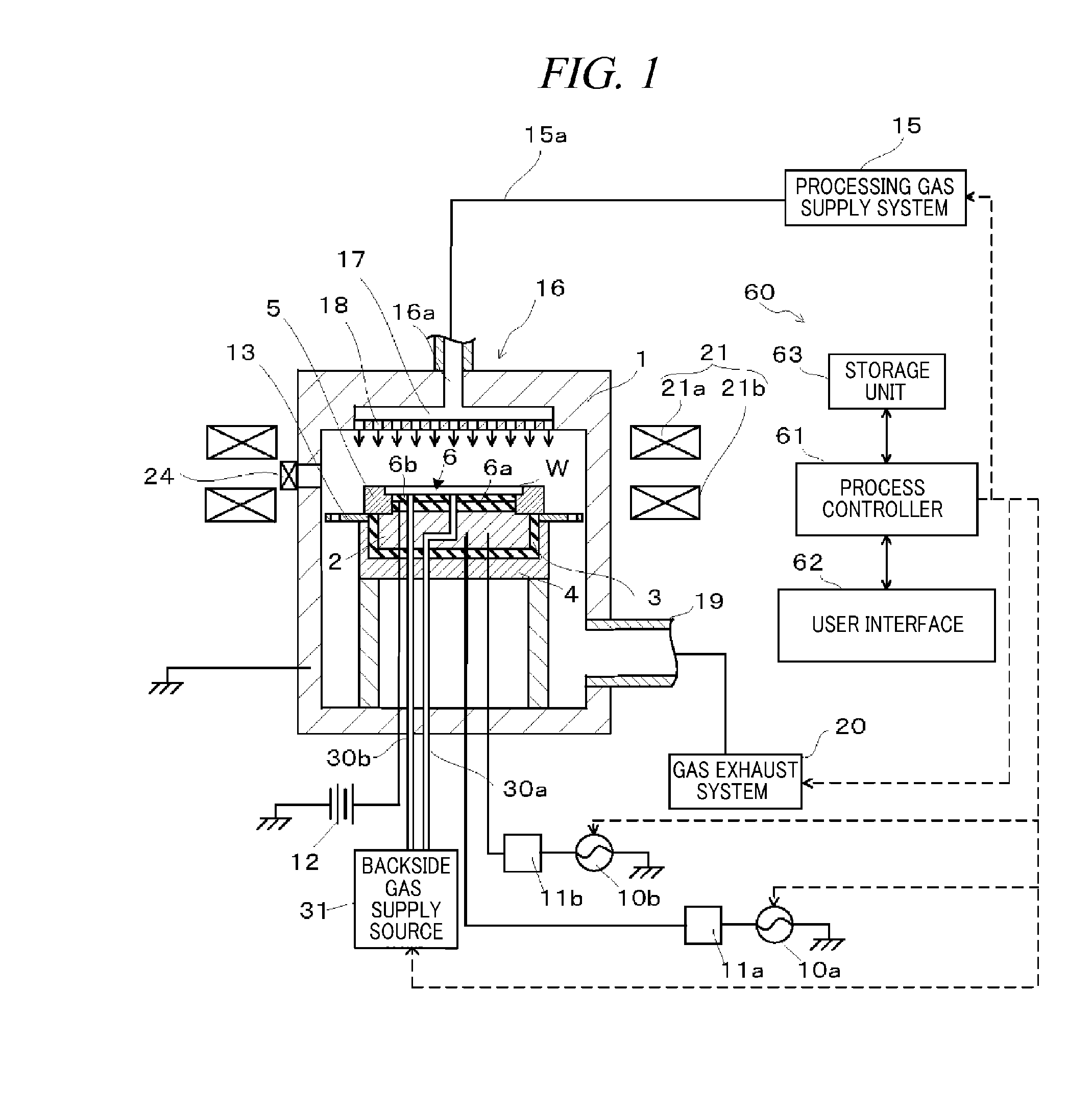
[0014]Hereinafter, illustrative embodiments will be described with reference to the accompanying drawings. FIG. 1 is a cross sectional view schematically illustrating a configuration of a plasma processing apparatus used in a semiconductor device manufacturing method in accordance with an illustrative embodiment. The plasma processing apparatus includes a processing chamber 1 that is hermetically sealed and electrically grounded.

[0015]The processing chamber 1 has a cylindrical shape and is made of, but not limited to, aluminum whose surface is coated with an anodic oxidized film. A mounting table 2 for horizontally mounting thereon a semiconductor wafer W as a processing target substrate is provided within the processing chamber 1. The mounting table 2 serves as a lower electrode and is made of a conductive material such as aluminum. The mounting table 2 is supported on a conductive support 4 via an insulating plate 3. Further, a circular ring-shaped focus ring 5 is placed on an upp...


PUM

PropertyMeasurementUnit
Internal pressureaaaaaaaaaa
Electrical conductoraaaaaaaaaa

Abstract

There is provided a semiconductor device manufacturing method for forming a step-shaped structure in a substrate by etching the substrate having thereon a multilayer film and a photoresist film on the multilayer film and serving as an etching mask. The multilayer film is formed by alternately layering a first film having a first permittivity and a second film having a second permittivity different from the first permittivity. The method includes a first process for plasma-etching the first film by using the photoresist film as a mask; a second process for exposing the photoresist film to hydrogen-containing plasma; a third process for trimming the photoresist film; and a fourth process for etching the second film by using the trimmed photoresist film and the plasma-etched first film as a mask. The step-shaped structure is formed in the multilayer film by repeatedly performing the first process to the fourth process in this sequence.

Description

CROSS-REFERENCE TO RELATED APPLICATION[0001]This application claims the benefit of Japanese Patent Application Nos. 2011-046772 and 2012-033954 filed on Mar. 3, 2011 and Feb. 20, 2012, respectively, and U.S. Provisional Application Ser. No. 61 / 466,192 filed on Mar. 22, 2011, the entire disclosure of which are incorporated herein by reference.FIELD OF THE INVENTION[0002]The present disclosure relates to a semiconductor device manufacturing method and a computer-readable storage medium.BACKGROUND OF THE INVENTION[0003]Conventionally, in a semiconductor device manufacturing process, various plasma processes such as an etching process and a film forming process are performed on a substrate such as a semiconductor wafer by using plasma. In such a semiconductor device manufacturing process, e.g., in a manufacturing process of a NAND type flash memory, it has been known to form a step-shaped structure by performing a plasma etching process and a mask trimming process on a multilayer film t...

Claims


Application Information

Patent Timeline
IPC IPC(8): H01L21/3065B05C21/00
CPCH01J37/32091H01J37/32669H01L21/0206H01L21/0273H01L21/31116H01L27/11582H01L21/31144H01L21/32137H01L21/32139H01L27/11556H01L21/31138H10B41/27H10B43/27
Inventor WATANABE, SEIICHISATO, MANABUNARISHIGE, KAZUKISATO, TAKANORIKATSUNUMA, TAKAYUKI
Owner TOKYO ELECTRON LTD
Why Eureka
Try Eureka