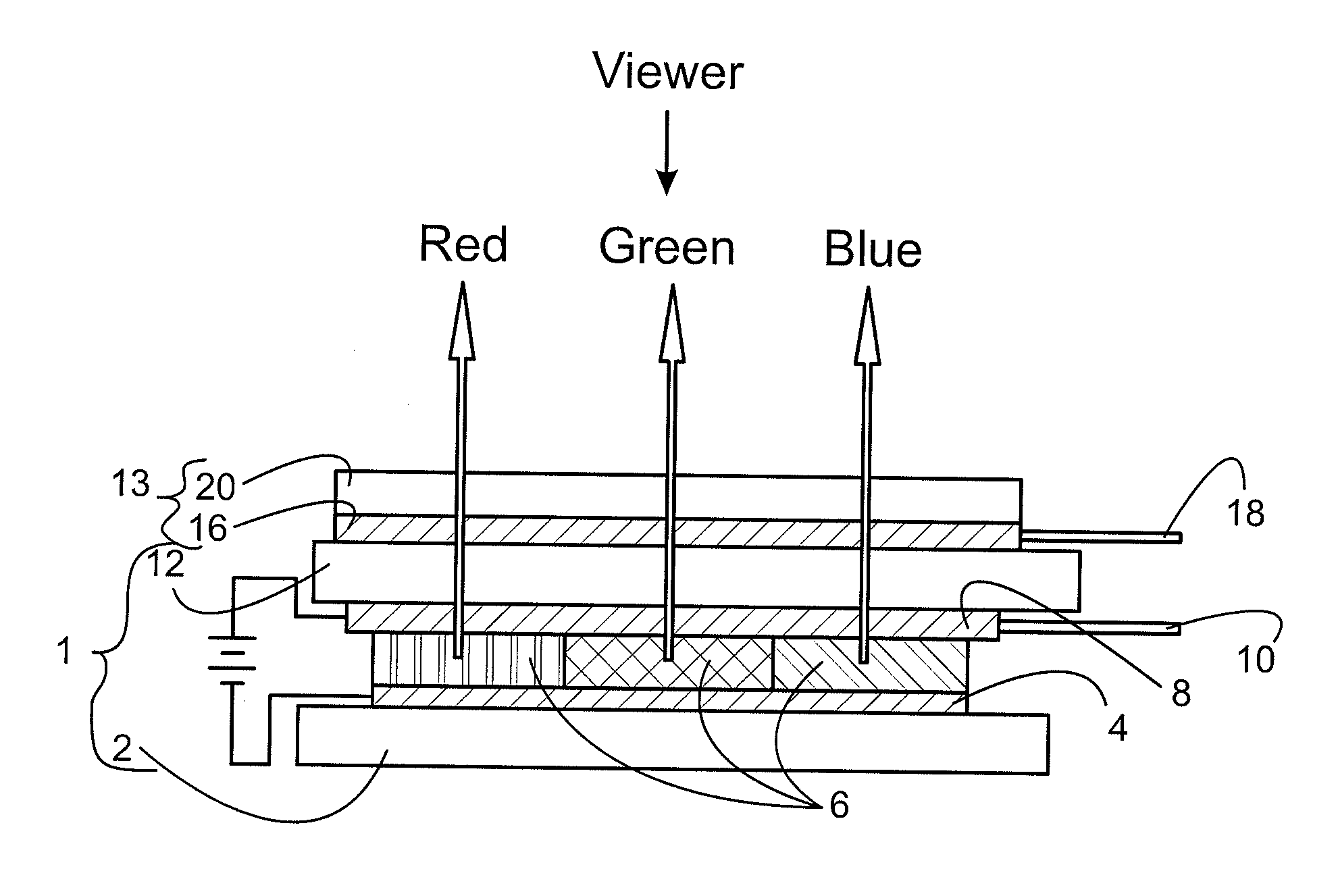
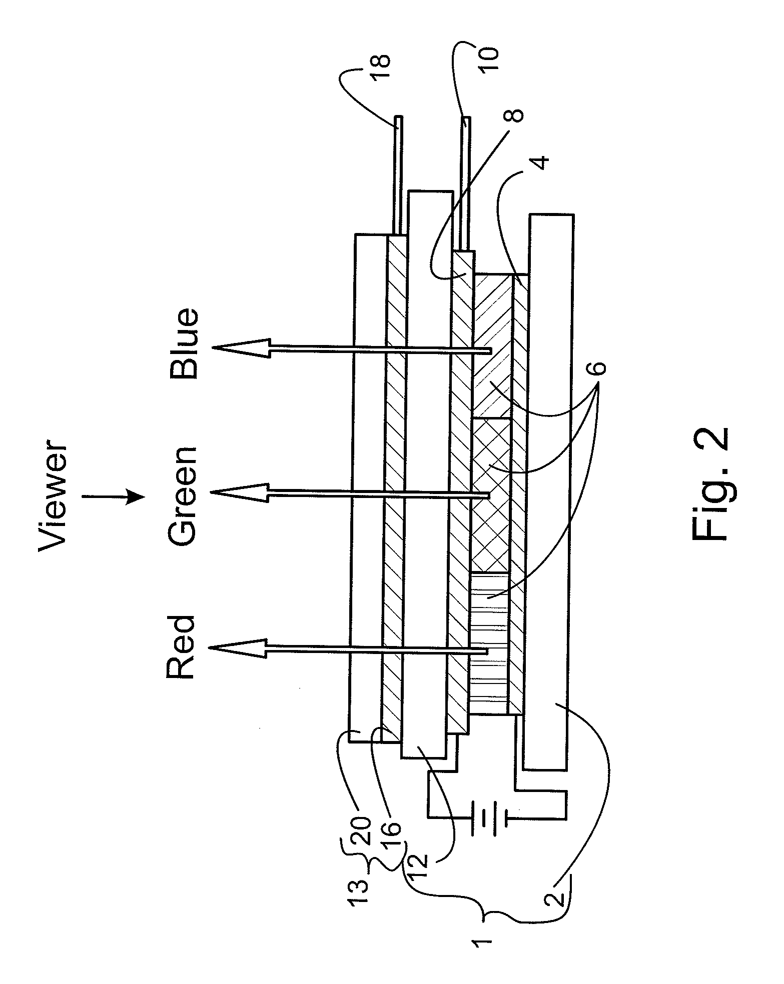
[0014]A product according to the present invention is a touch screen on a display device having an upper substrate for protecting the display device from the environment, the touch screen comprising an
electrically conductive transparent first layer. The first layer comprises a network of electrically conductive high
aspect ratio molecular structures (HARM-structures), the first layer being embedded into the upper substrate of the display device to protect the conductive transparent first layer, for reducing the optical thickness of the structure between a viewer and the region of the display device in which the image is formed.
[0015]A method according to the present invention, for manufacturing a touch screen on a display device having an upper substrate for protecting the display device from the environment, comprises the steps of depositing an electrically conductive transparent first layer comprising a network of electrically conductive high
aspect ratio molecular structures (HARM-structures) on the upper substrate of the display device in contact with the upper substrate, and pressing the first layer against the upper substrate, to embed the first layer into the upper substrate, for reducing the optical thickness of the structure between a viewer and the region of the display device in which the image is formed.
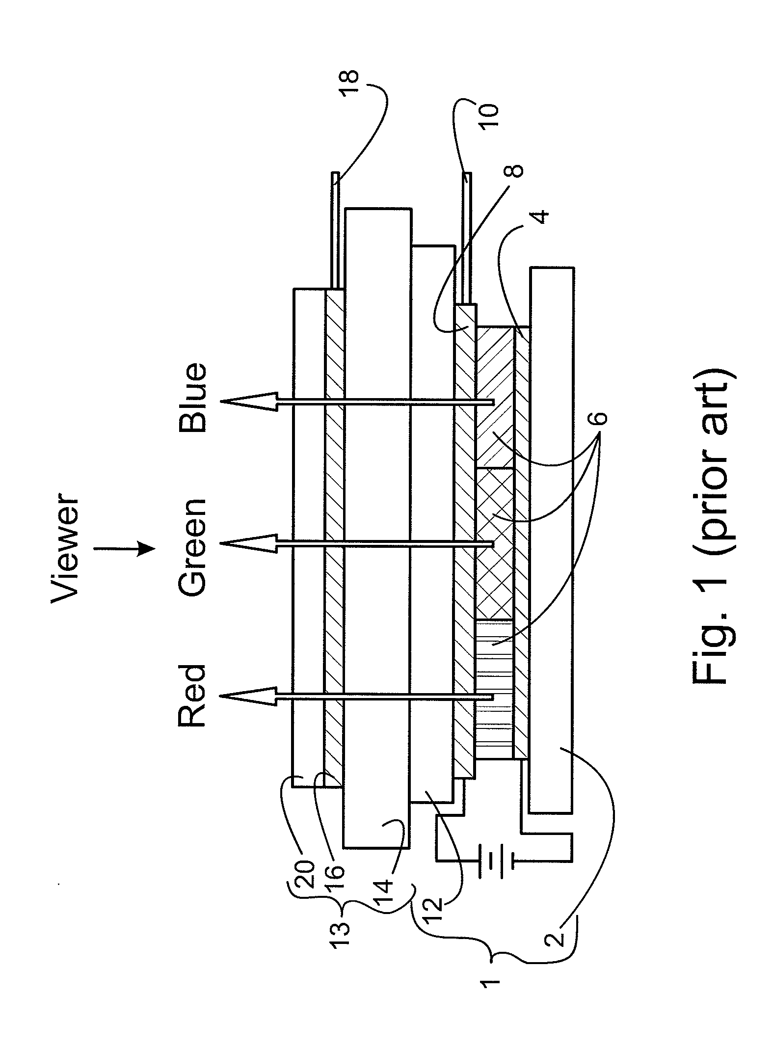
[0018]Depositing the first layer on the upper substrate of the display device, such that the first layer resides in contact with the upper substrate, removes the need for using a dedicated substrate for depositing the first layer. This results in an optically thin design for the touch screen on the display, which improves the
readability of the display under the touch screen and, therefore, the
usability of the touch display. It furthermore simplifies the design and fabrication process of the whole structure as the touch screen can now be directly fabricated on the display device with good electrical and
optical quality. Mechanical durability of networks of HARM-structures also results in additional advantages for the end product and enables more reliable manufacturing of the touch display. Moreover, as networks of HARM-structures need not be continuous to be conductive throughout the area of the network, as opposed to e.g. films of
metal oxides such as ITO, the deposited networks of HARM-structures can be exceptionally thin while being mechanically and electrically robust. This enables the deposition of very thin networks of HARM-structures with good electrical and mechanical properties for touch screen applications, which increases transparency of the touch screen structure and thereby improves the quality of the image through the touch screen, as experienced by the user.
[0025]An additional benefit in some embodiments of the invention is that the first layer, i.e. the network of HARM-structures, can be protected from the environment by embedding the network into the upper substrate of the display device. A network of interconnected HARM-structures is flexible and mechanically durable. This enables embedding the network of HARM-structures into the upper substrate by e.g. thermo-compression. In thermo-compression the upper substrate, which can be of e.g.
polymer, is first softened by
thermal treatment and subsequently the network of HARM-structures is pressed against the softened upper substrate to transfer the first layer into the upper substrate. When the first layer is encapsulated in the upper substrate in some embodiments of the invention, there is no longer a need to apply additional protective coatings on or under the first layer, which enables touch screen structures with small optical thickness to be fabricated. This further improves the
readability and
optical quality /
usability of the touch display.
[0028]In one embodiment of the present invention the network of high aspect ratio molecular structures (HARM-structures) is a network of carbon nanotubes. In one embodiment of the present invention the network of high aspect ratio molecular structures (HARM-structures) is a network of carbon nanobud molecules having a
fullerene molecule covalently bonded to the side of a tubular carbon molecule. Carbon nanotubes (CNTs) and carbon nanobuds (CNBs) are examples of HARM-structures which, when deposited on a substrate, can form a mechanically flexible and durable network which is electrically very conductive even when the deposit is very thin and transparent. Therefore these HARM-structures are well suited for the conductive transparent
layers employed in touch screens. Networks of CNTs or CNBs furthermore possess a low
refractive index which adds to their potential applicability to touch screens with a small optical thickness. Networks of CNTs or CNBs also exhibit a high charge storage capacity. This additional
advantage, with the good electrical
conductivity, can be put to use in capacitive and projective capacitive touch screens, to enable shorter response times for registering a touch on the touch screen.
[0029]In one embodiment of the invention the touch screen comprises a top substrate layer on the first layer, to protect the first layer from the environment. Under harsh operating conditions where the touch screen becomes exposed to e.g. large temperature variations, a chemically aggressive environment or repeated mechanical stress a top substrate layer may be utilized to provide additional protection for the first layer even when the first layer is embedded into the upper substrate of the display device.


